Analog building block
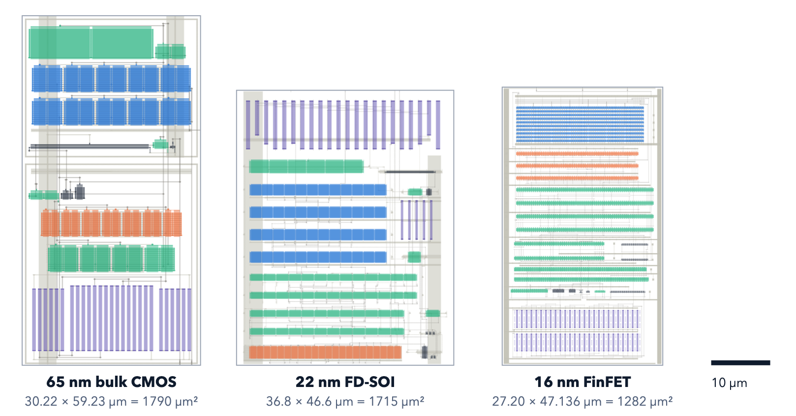
A current reference across three processes.
Two nominal 10-µA outputs from an untrimmed temperature-compensated architecture implemented in bulk CMOS, FD-SOI and FinFET.
Results at a glance
The same untrimmed current-reference architecture, implemented in three technologies.
Physical sign-off
DRC, LVS, antenna, density and latch-up checks.
Reliability review
Electromigration, IR drop, redundant supply vias and gate-oxide voltage.
Extracted-layout verification
PVT, process-plus-mismatch Monte Carlo and start-up verification.
| Measure | 65-nm bulk CMOS | 22-nm FD-SOI | 16-nm FinFET |
|---|---|---|---|
| Supply | 1.2 V | 0.8 V | 0.8 V |
| Typical output | 10.06 µA | 10.03 µA | 9.73 µA |
| Drawn macro area | 1,790 µm² | 1,715 µm² | 1,282 µm² |
| Untrimmed 3σ accuracy | ±17.87% | ±20.84% | ±18.70% |
| Typical temperature coefficient | 58 ppm/°C | 38 ppm/°C | 58 ppm/°C |
| Own power, excluding two outputs | 14.2 µW | 18.0 µW | 8.5 µW |
All electrical values are post-layout simulation with extracted parasitics, not silicon measurements. Accuracy is untrimmed process-plus-mismatch Monte Carlo; see page 06 for limits and modelling basis.
How the reference works
Opposing temperature trends are weighted into a nearly flat current.
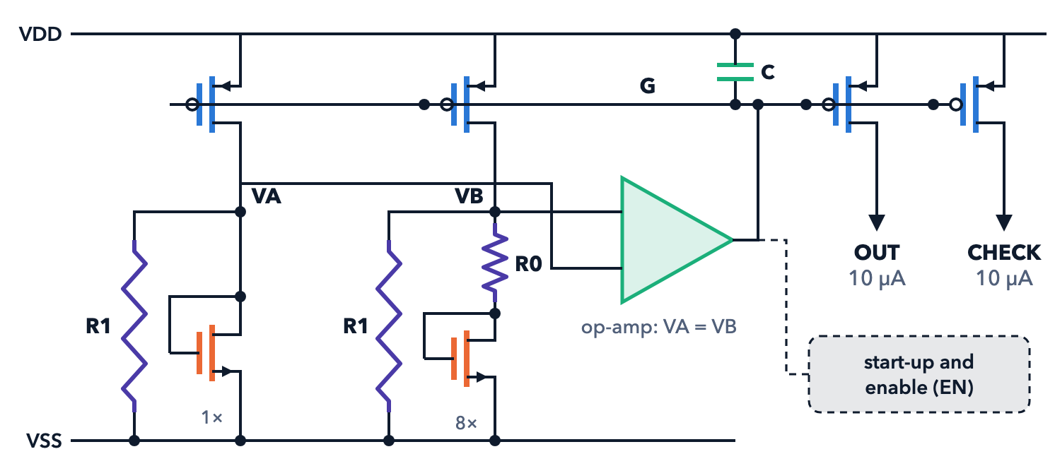
- The op-amp holds VA = VB; a PMOS mirror produces two nominal 10-µA copies: OUT feeds the bias generator and CHECK is a spare reference-check output.
- A weak pull-up starts the self-biased loop. EN switches the whole reference off. Node-specific adaptations include 22-nm output clamps and short-unit resistor and gate structures at 16 nm.
- A beta-multiplier alternative was simulated and rejected: 65-nm corners reached −18.2/+25.9% against ±20%; 22- and 16-nm temperature coefficients exceeded 1194 and 1461 ppm/°C against a 300-ppm/°C limit.
65-nm physical implementation
Bulk-CMOS layout, 30.22 × 59.23 µm = 1,790 µm².
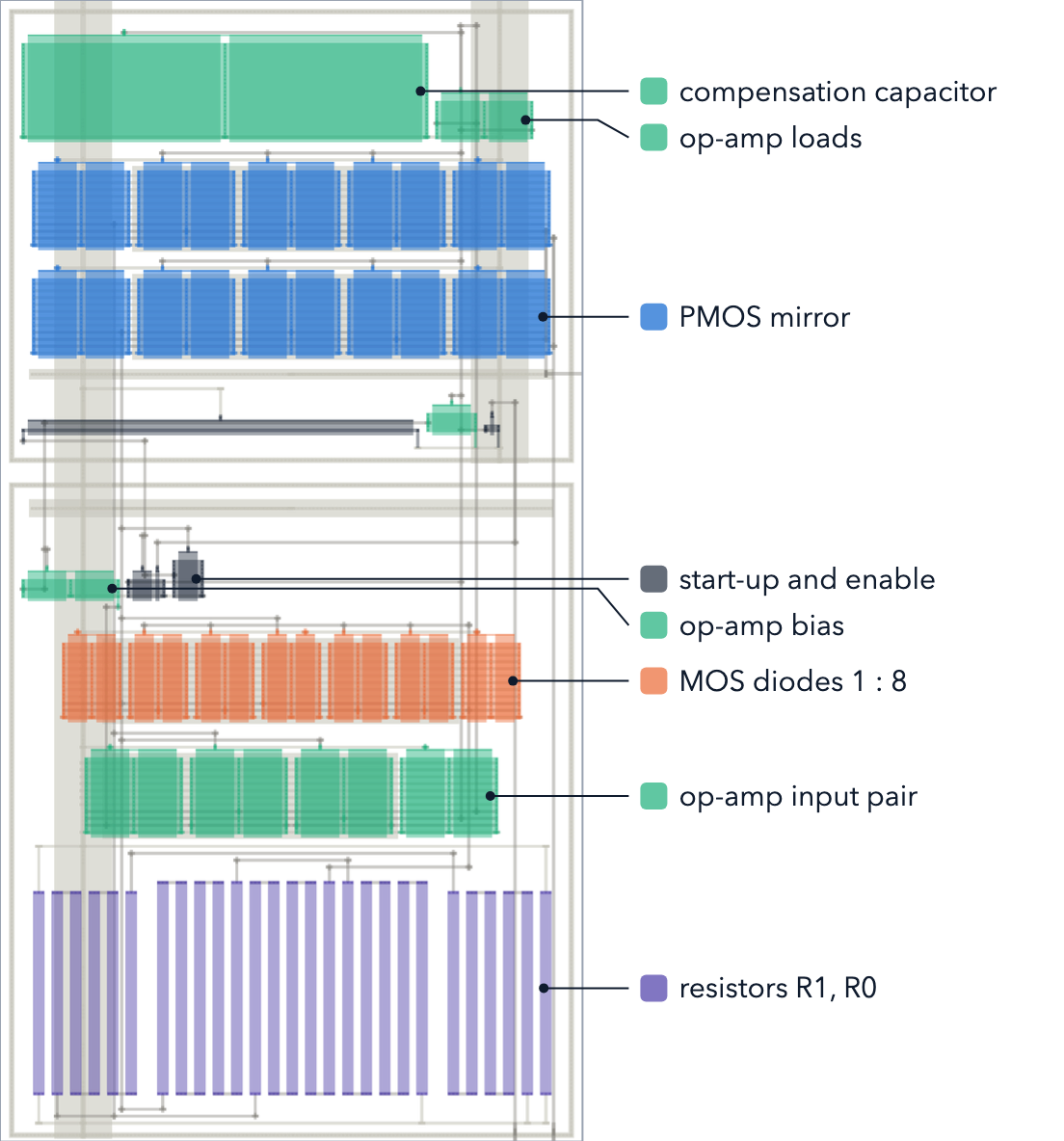
- Matched PMOS mirror includes two branches and two output copies; MOS diodes use a 1:8 ratio; the op-amp input pair is matched.
- Each matched group uses end dummies and identical neighbours and sits at least 5 µm from a well edge.
- R1 and R0 are parallel poly strips of one width. Supply is 1.2 V.
22-nm physical implementation
FD-SOI layout, 36.8 × 46.6 µm = 1,715 µm².
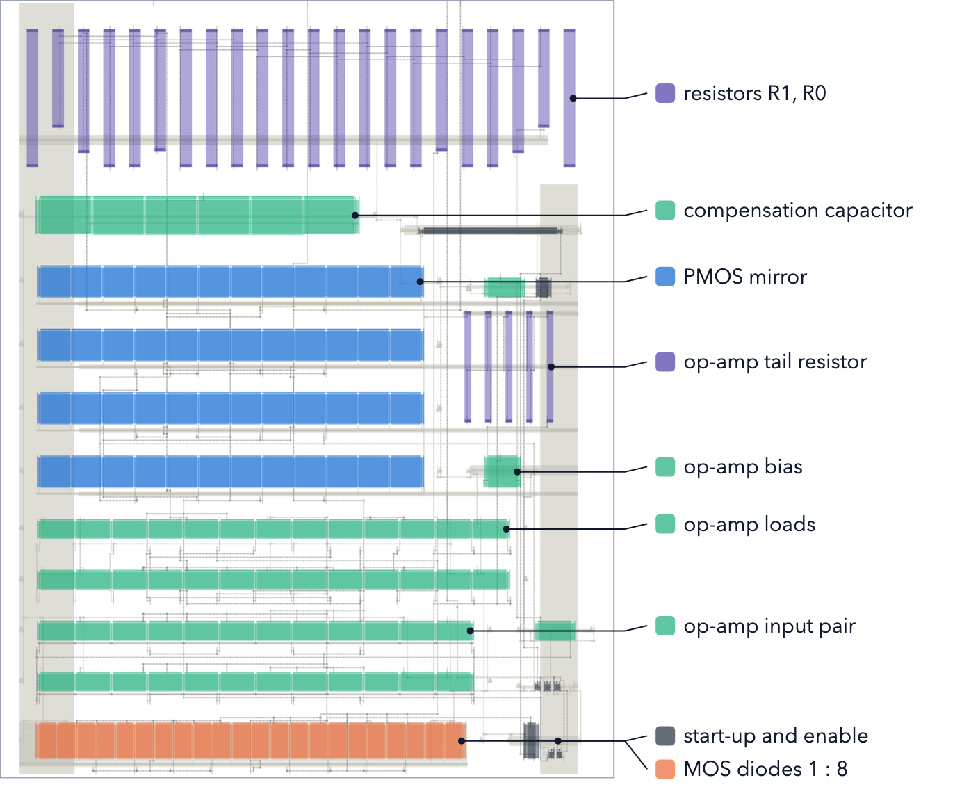
- Continuous diffusion rows put each device centroid at the array centre (0.0-µm offset): 32-finger PMOS mirror, 18 diode devices, 16 op-amp input devices and 16 loads.
- R1 and R0 use interleaved unit strips with end dummies.
- The two-dummy row ends are an owner-approved exception to longer saturating dummies; its measured cost is included in the reported results. Supply is 0.8 V.
16-nm physical implementation
FinFET layout, 27.20 × 47.136 µm = 1,282 µm².
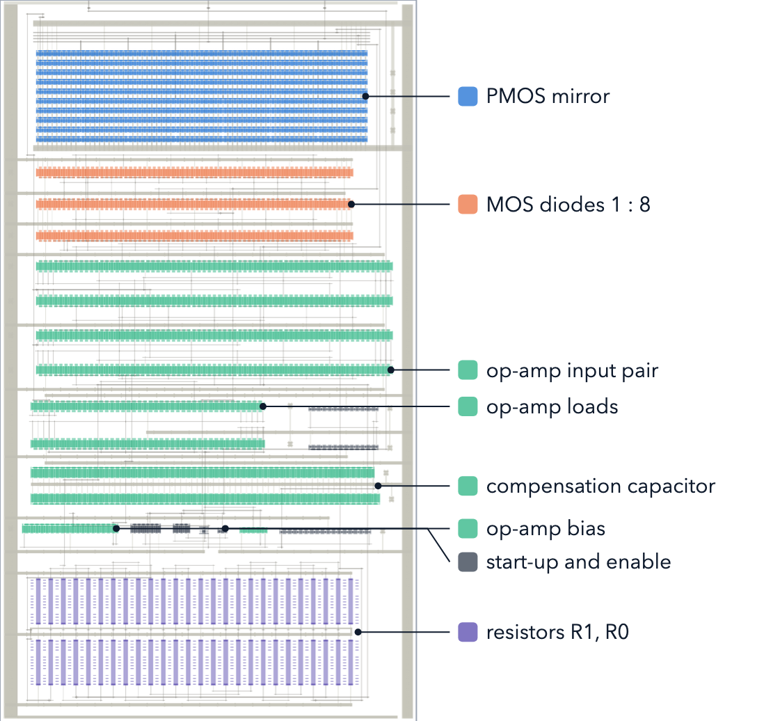
- PMOS mirror: eight rows and 96 units. Diodes at 1:8 ratio use three rows; the op-amp pair uses four rows. Matched-group centroids have 0.0-µm offset.
- R1 and R0 use 47 identical units in a 2 × 26 interleaved array with dummies.
- Process rules led to short-unit resistors and stacked short-gate devices. Supply is 0.8 V.
Untrimmed accuracy
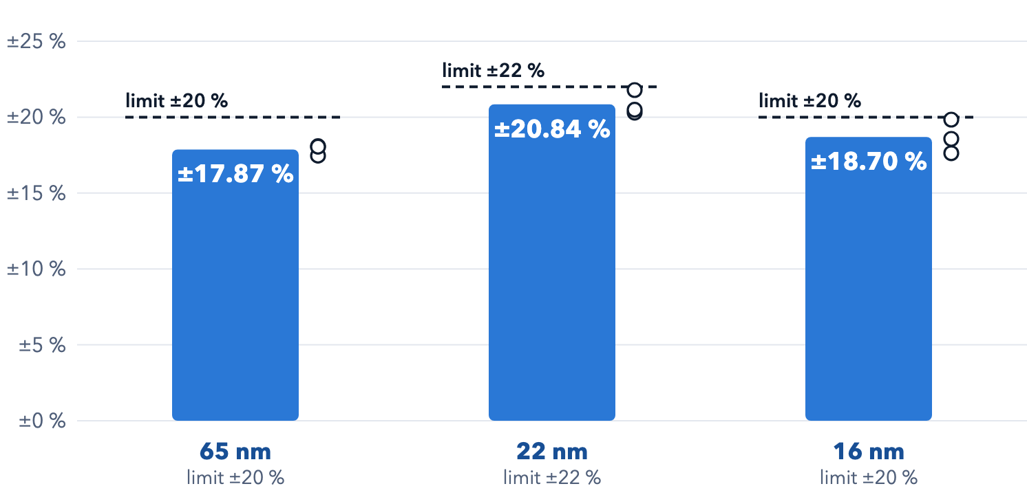
Process-plus-mismatch Monte Carlo on extracted layouts at tt, 27 °C and nominal supply.
| Technology | Process σ | Mismatch σ | Pooled 3σ | 3σ by seed | Limit |
|---|---|---|---|---|---|
| 65-nm bulk | 5.63% | 1.93% | ±17.87% | 18.09 / 17.46 / 18.05% | ±20% |
| 22-nm FD-SOI | 6.69% | 1.89% | ±20.84% | 20.30 / 21.78 / 20.49% | ±22% |
| 16-nm FinFET | 5.56% | 2.82% | ±18.70% | 17.63 / 19.84 / 18.57% | ±20% |
Three seeds of 200 process plus 200 mismatch runs each; pooled 3σ = 3 × √(process σ² + mismatch σ²). 22-nm accuracy uses the technology’s best-case mismatch model, the design basis; the worst-case model gives ±25.9%. The 65-nm process runs were added for this presentation; its sign-off checked the 45-point corner box and mismatch σ.
Temperature stability
Output current from 0 to 85 °C relative to 27 °C, at nominal supply.
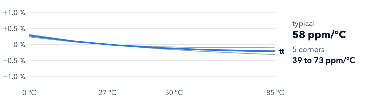
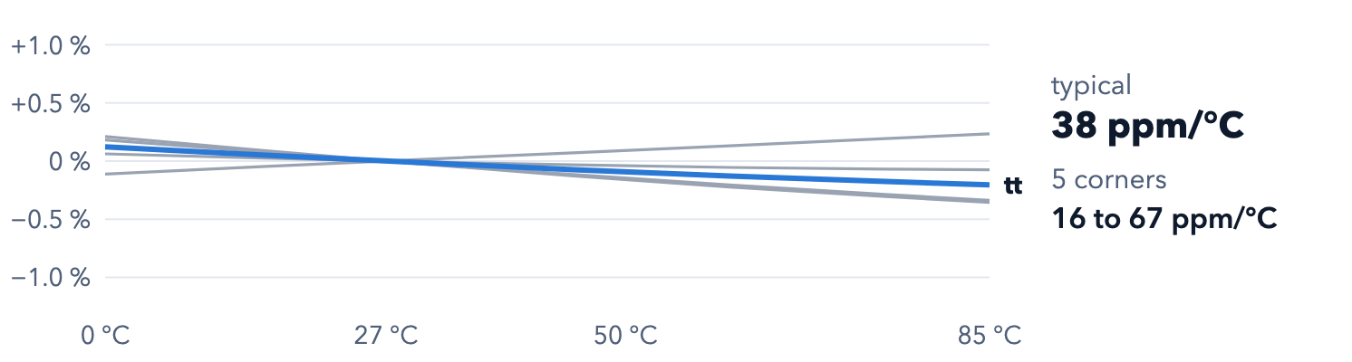
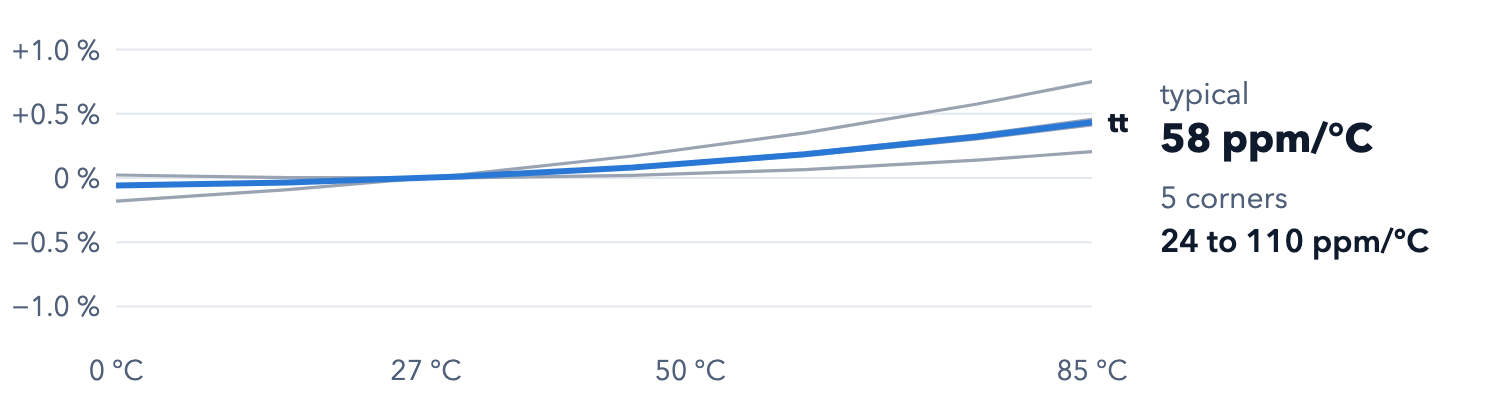
Blue shows the typical process; grey shows four other process corners. The acceptance limit is 300 ppm/°C. Temperature coefficient is the largest-to-smallest current span, divided by the 27 °C current and by 85 K.
Reliable start-up
The circuit must leave its zero-current state for fast and slow supply ramps.
| Technology | Passing cases | Conditions | Settled to 1% |
|---|---|---|---|
| 65-nm bulk | 135 / 135 | 45 PVT points × 1-ns step, 10-µs ramp, 1-ms ramp; extracted reference + bias generator | ≤0.68 µs |
| 22-nm FD-SOI | 135 / 135 schematic; 3 / 3 extracted | Three near-latch corners post-layout with all supply ramps; no second state in 1000 Monte Carlo runs | ≤0.36 µs |
| 16-nm FinFET | 93 / 93 | 45 PVT points × step and 10-µs ramp; 1-ms ramp at three points; extracted reference + bias generator | ≤0.689 µs |
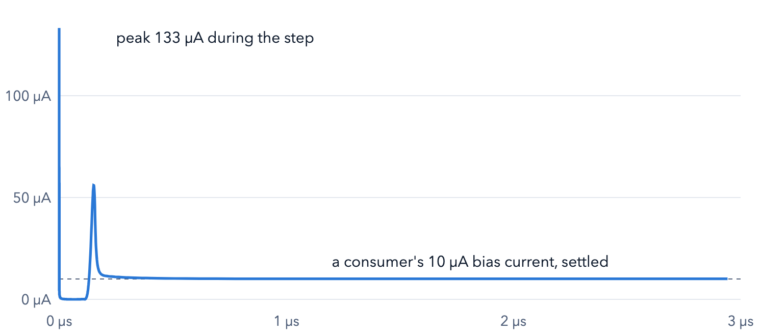
Settling is measured after the supply step, within 1% of final current. At system integration, consumer blocks are enabled at least 2 µs after the reference.
Performance summary
Key extracted-layout metrics from the final public results; worst case across 45 PVT points unless noted.
| Measure | 65-nm bulk | 22-nm FD-SOI | 16-nm FinFET |
|---|---|---|---|
| Area | 1,790 µm² | 1,715 µm² | 1,282 µm² |
| Supply ±5% | 1.2 V | 0.8 V | 0.8 V |
| Output, typical | 10.06 µA | 10.03 µA | 9.73 µA |
| Accuracy, untrimmed 3σ | ±17.87% (limit ±20%) | ±20.84% (limit ±22%) | ±18.70% (limit ±20%) |
| Process corners, 45 PVT points | −8.6 / +13.4% | −11.6 / +16.1% | −12.3 / +12.6% |
| TC, tt (corner range) | 58 (39–73) ppm/°C | 38 (16–67) ppm/°C | 58 (24–110) ppm/°C |
| Line regulation | ≤0.49 %/V | ≤0.72 %/V | ≤0.26 %/V |
| PSRR at DC, worst | 42.1 dB | 44.0 dB | 49.9 dB |
| Own power, typical | 14.2 µW | 18.0 µW | 8.5 µW |
| Start-up | 135/135 cases | 3/3 extracted near-latch corners | 93/93 cases |
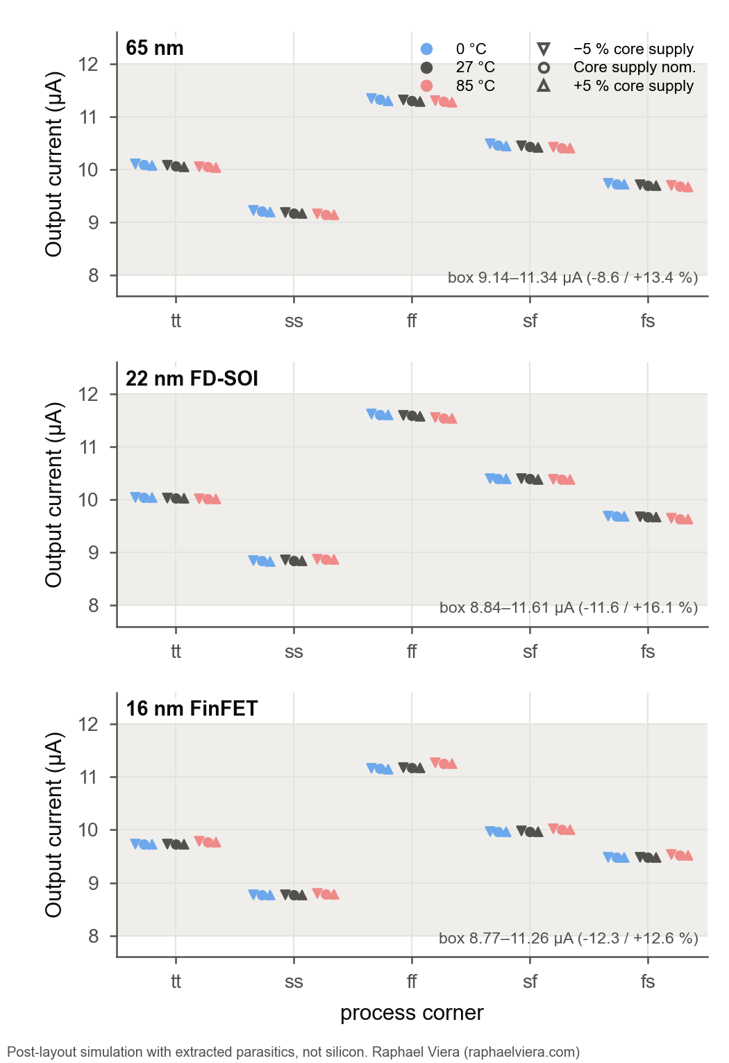
Own power excludes the two output currents. The 22-nm 3σ figure uses the best-case mismatch model. Line regulation is the 27-°C per-corner measure; PSRR is normalized DC worst-of-box. These are post-layout simulations with extracted parasitics, not silicon.
Values are post-layout simulation with extracted parasitics, not silicon measurements. · Raphael Viera (raphaelviera.com)