| [1] | M. A. P. Pertijs et al. | JSSC | 2005 | 0.7 um CMOS | Substrate PNP, VBE/dVBE (5:1 bias)†, 2nd-order SC ΔΣ; full sensor | 4.5 mm^2 (chip)† | 75 uA, 2.5-5.5 V† | -55 to 125 | ±0.1 (3σ, 1-pt trim at 30 C†, N=24†) | 0.01 C rms at 10 conv/s† | 10 conv/s† | Meas., 24† | 10.1109/JSSC.2005.858476 | abstract + ISSCC'05 digest full text† |
|---|
| [2] | K. Souri et al. | JSSC | 2013 | 0.16 um CMOS | PNP, VBE/dVBE, zoom ADC (5b SAR + 10b ΔΣ); decimation off-chip | 0.08 mm^2 | 3.4 uA @1.5-2 V (excl. off-chip digital) | -55 to 125 | ±0.15 (3σ, batch cal + RT voltage cal + PTAT trim, N=18); ±0.25 (lot 2, N=18 ceramic + 22 plastic); ±0.6 batch cal only | 20 mK rms (5 mK in 100 ms) | 5.3 ms | Meas., 18+18+22 | 10.1109/JSSC.2012.2214831 | full text |
|---|
| [3] | A. Heidary et al. | ISSCC | 2014 | 0.7 um CMOS‡ | BJT (substrate PNP‡), CT duty-cycle-modulated output | die 1.7 x 1.3 mm‡ | 200 uW (60 uA @3.3 V)‡ | -45 to 130 | spread < ±0.15 (3σ, single RT trim, N n/s) | 3 mK | 2.2 ms | Meas. | 10.1109/ISSCC.2014.6757410 | abstract + TIE'17 full text‡ |
|---|
| [4] | B. Yousefzadeh et al. | JSSC | 2017 | 0.16 um CMOS | Substrate PNP, zoom ADC; digital off-chip | 0.16 mm^2 (core) | 4.6 uA @1.8 V nom. (1.5-2 V) | -55 to 125 | ±0.06 (3σ, batch cal + RT PTAT trim, N=20); ±0.1 (3σ, common params + 1-pt, N=80 / 3 batches) | 15 mK rms | 5 ms | Meas., 20 / 80 | 10.1109/JSSC.2016.2638464 | full text (accepted manuscript) |
|---|
| [5] | B. Yousefzadeh and K. A. A. Makinwa | JSSC | 2020 | 0.16 um CMOS | PNP, low-leakage SC ADC + on-chip heater | 0.15 mm^2 (incl. 0.017 mm^2 heater; TDC 0.05 mm^2) | 5.41 uA @1.8 V (9.75 uW) | -40 to 180 | ±0.25 (3σ, heater-assisted 2-pt voltage cal, N=24); ±0.2 (3σ, 1-pt temperature trim) | 23 mK rms | 20 ms | Meas., 24 | 10.1109/JSSC.2019.2953834 | full text |
|---|
| [6] | Z. Tang et al. | JSSC | 2023 | 0.18 um CMOS | PNP, capacitively biased, SC ΔΣ with inverter-based integrators; sinc2 off-chip | 0.25 mm^2 | 810 nW @0.95 V (RT) | -55 to 125 | ±0.15 (3σ, 1-pt PTAT trim, N=20); ±0.45 batch cal only | 1.8 mK rms | 128 ms | Meas., 20 | 10.1109/JSSC.2023.3308554 | full text |
|---|
| [7] | N. G. Toth and K. A. A. Makinwa | JSSC | 2024 | 0.18 um CMOS | NPN, beta-compensated current-mode front end, CT ΔΣ | 0.07 mm^2 | 2.5 uA @1.4 V (1.4-2.2 V) | -55 to 125 | ±0.1 (3σ, RT trim + resistor-ratio cal, N=40 on 20 dies)§; ±0.2 RT trim only; ±0.25 voltage cal | 1.2 mK rms | 38.4 ms | Meas., 40 | 10.1109/JSSC.2024.3440071 | full text |
|---|
| [8] | N. G. Toth et al. | JSSC | 2025 | 0.18 um CMOS | PNP, resistor V-to-I front end, CT ΔΣ | 0.12 mm^2 (per sensor) | 9.5 uA @1.7 V (1.7-2.2 V) | -55 to 125 | ±0.1 (3σ, RT trim + resistor-ratio cal, N=40 on 20 dies)§; ±0.17 RT trim only, or voltage cal | 1.1 mK rms | 40 ms | Meas., 40 | 10.1109/JSSC.2024.3402131 | full text |
|---|
| [9] | N. G. Toth and K. A. A. Makinwa | ISSCC | 2025 | n/s | NPN, charge-balancing CT ΔΣ | 0.05 mm^2 | | -70 to 125 | 0.1 (3σ, trim n/s, N n/s) | | | Meas. | 10.1109/ISSCC49661.2025.10904777 | abstract only |
|---|
| [10] | F. Sebastiano et al. | JSSC | 2010 | 65 nm CMOS | Vertical NPN (deep n-well collector), SC ΔΣ; decimation off-chip | 0.1 mm^2 (active) | 8.3 uA @1.2 V (title: 10 uW) | -70 to 125 | ±0.2 (3σ, 1-pt trim at 30 C, N=16); ±0.5 (3σ, batch cal, N=12) | 0.03 C (quantization-limited) | 2.2 Sa/s | Meas., 12 / 16 | 10.1109/JSSC.2010.2076610 | full text (author draft)* |
|---|
| [11] | J. S. Shor and K. Luria | JSSC | 2013 | 32 nm and 22 nm CMOS | BJT; BJT voltage and reference each converted to frequency, ratio taken digitally | 0.02 mm^2 (32 nm) / 0.006 mm^2 (22 nm), incl. all digital | 3.8 mW / 1.4 mW @1.4 V (unregulated) | | | ±0.2 C rms (as written) | 2-20 kS/s | Meas. | 10.1109/JSSC.2013.2280039 | abstract only |
|---|
| [12] | T. Oshita et al. | JSSC | 2015 | 14 nm tri-gate (FinFET) CMOS | BJT, compact processor hot-spot sensor | 0.0087 mm^2 | 1.1 mW | | | 0.5 C | > 50 kS/s | Meas. | 10.1109/JSSC.2015.2396522 | abstract only |
|---|
| [13] | M. Eberlein and I. Yahav | VLSI | 2016 | 28 nm CMOS | Parasitic NPN, current mode, 8 b | 0.0038 mm^2 | 16 uA @1.8 V | -20 to 130 | 1.8 (3σ, no calibration); ~±0.8 (1-pt soft trim) | | | Meas. | 10.1109/VLSIC.2016.7573532 | abstract only |
|---|
| [14] | Y.-C. Hsu et al. | ISSCC | 2017 | n/s* | Dynamic-distributing-bias sensor (device n/s in abstract) | 0.00946 mm^2 | 18.75 uW | | 0.87 (3σ, untrimmed; title); relative 1.64 % (abstract)* | | | Meas. | 10.1109/ISSCC.2017.7870281 | abstract only |
|---|
| [15] | D. S. Lin and H. P. Hong | A-SSCC | 2017 | 10 nm FinFET | BJT, charge pump for 0.5 V operation, SC-integrator V-to-f | 0.01 mm^2 | 125 uW @0.5 V | | ±2.8 (3σ spread at 85 C only; trim n/s) | ±0.173 C rms (as written) | | Meas. | 10.1109/ASSCC.2017.8240211 | abstract only |
|---|
| [16] | C.-Y. Lu et al. | ISSCC | 2018 | 22 nm FinFET | Hybrid parasitic PNP + subthreshold NMOS, current mode, 8 b; single-element remote PNP (0.00021 mm^2) + one wire to the main sensor | 0.0043 mm^2 (system) | 50 uA @1 V | | ±1.07 (±3σ, 1-pt voltage-based soft trim) | | | Meas. | 10.1109/ISSCC.2018.8310312 | abstract only |
|---|
| [17] | Z. Tang et al. | TCAS-II | 2019 | 55 nm CMOS | Substrate BJT, current mode, dynamic beta compensation | 0.0146 mm^2 | 37 uW | -40 to 125 | ±1.7 (3σ, untrimmed) | 12-15 bit (adjustable) | 4.1-32.8 ms | Meas. | 10.1109/TCSII.2019.2921889 | abstract only |
|---|
| [18] | M. Eberlein and H. Pretl | ESSCIRC | 2019 | 16 nm FinFET | Bulk diodes, NOT BJT*; charge-pump biased; capacitive SAR charge balancing | 2500 um^2 (active) | 230 pJ/conversion (power n/s); down to 0.85 V | consumer range (no numbers) | +1.5/-2.0 (min/max, no calibration) | | 12.8 us | Meas. | 10.1109/ESSCIRC.2019.8902928 | abstract only |
|---|
| [19] | Z. Tang et al. | JSSC | 2025 | 22 nm bulk CMOS | Parasitic PNP, capacitively biased via regulated charge pumps, charge-balancing ΔΣ; sinc2 off-chip | 0.01 mm^2 (core) | 2.9 uW @0.8 V (RT)* | -40 to 125 | ±0.4 (3σ, 1-pt offset trim, N=23); ±1.25 untrimmed | 4.7 mK rms (88 mK) | 6.4 ms (0.82 ms) | Meas., 23 | 10.1109/JSSC.2024.3523482 | full text |
|---|
| [20] | Y. Li et al. | JSSC | 2025 | 4 nm FinFET | Parasitic PNP + subthreshold MOS; dual temperature-sensor / sub-1-V BGR | 0.0061 mm^2 (stated as BGR footprint)* | 68.5 uW | | n/s in abstract | 0.46 C | 7 us | Meas. | 10.1109/JSSC.2024.3524245 | abstract only |
|---|
| [21] | X. Pu et al. | JSSC | 2015 | 65 nm digital CMOS | Remote BJTs (on PCB or in the SoC) read by an embedded sensor that shares an external reference with the SoC's other data converters; digital beta correction | | | -40 to 130 | 0.4 (3σ, trim n/s, N=16 with 4 BJTs) | | | Meas., 16 | 10.1109/JSSC.2015.2434845 | abstract only |
|---|
| [22] | O. Bass and J. Shor | TCAS-I | 2020 | 65 nm CMOS | PNP, switched-capacitor bandgap, 1-bit ΔΣ | 0.003 mm^2 | | | ±1.35 total (±3σ, digital trims, N n/s)* | 65 mK | 4.1 ms | Meas. | 10.1109/TCSI.2020.2987595 | abstract only |
|---|
| [23] | O. Bass and J. Shor | TCAS-II | 2020 | 65 nm CMOS | PNP, charge balancing; 50 um^2 sensing element | 1450 um^2 | | 150 C span | -2/+4 (p-p, 1-pt trim); -2.5/+1.5 (p-p, 2-pt trim) | 0.22 C | 821 us | Meas. | 10.1109/TCSII.2020.2999494 | abstract only |
|---|
| [24] | J.-H. Park et al. | JSSC | 2022 | 0.11 um CMOS | BJT core + relaxation-oscillator T-to-f converter (CTAT/PTAT ratio) | 0.025 mm^2 (active) | 3.1 uW | -40 to 140 | ±1 (3σ, "with the digital trimming", N=18)* | | | Meas., 18 | 10.1109/JSSC.2022.3182708 | abstract only |
|---|
| [25] | J. Yang et al. | TCAS-II | 2025 | 0.18 um CMOS | BJT, VBE2/VBE1 digitized directly by a 12-bit SAR ADC (no amplifier) | 0.02 mm^2 | 30 uA @1.8 V (RT) | -40 to 120 | ±0.6 (3σ, trim n/s, N n/s) | | 16 us | Meas. | 10.1109/TCSII.2025.3564315 | abstract only |
|---|
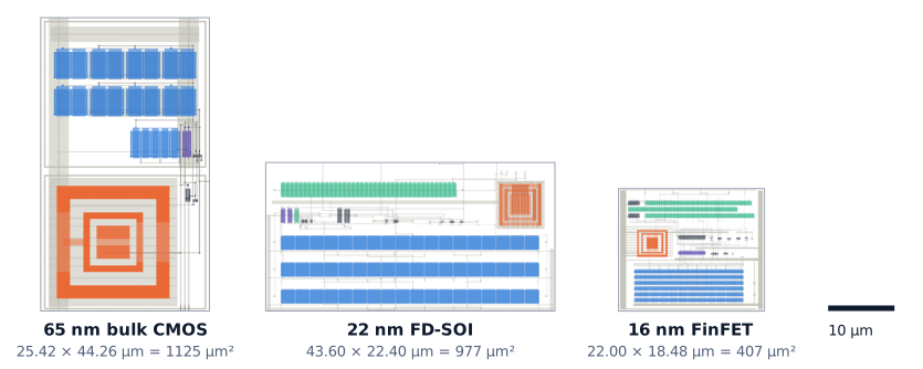
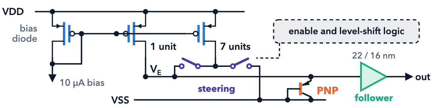
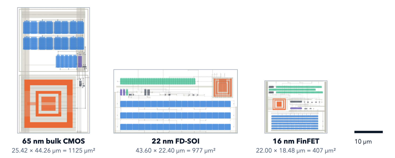
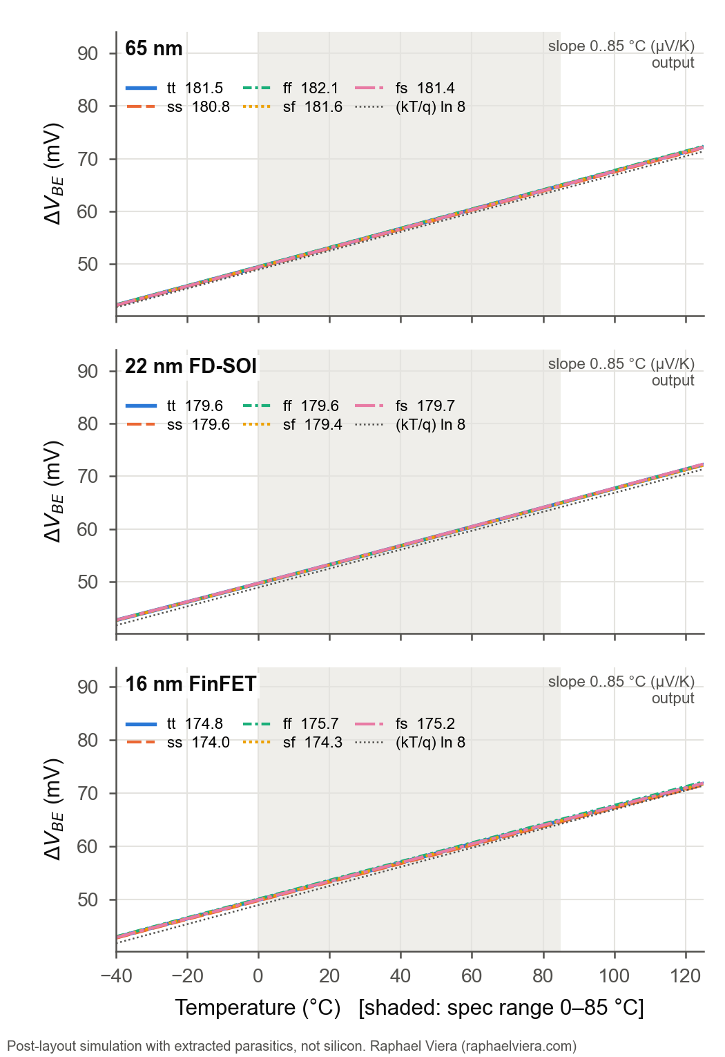
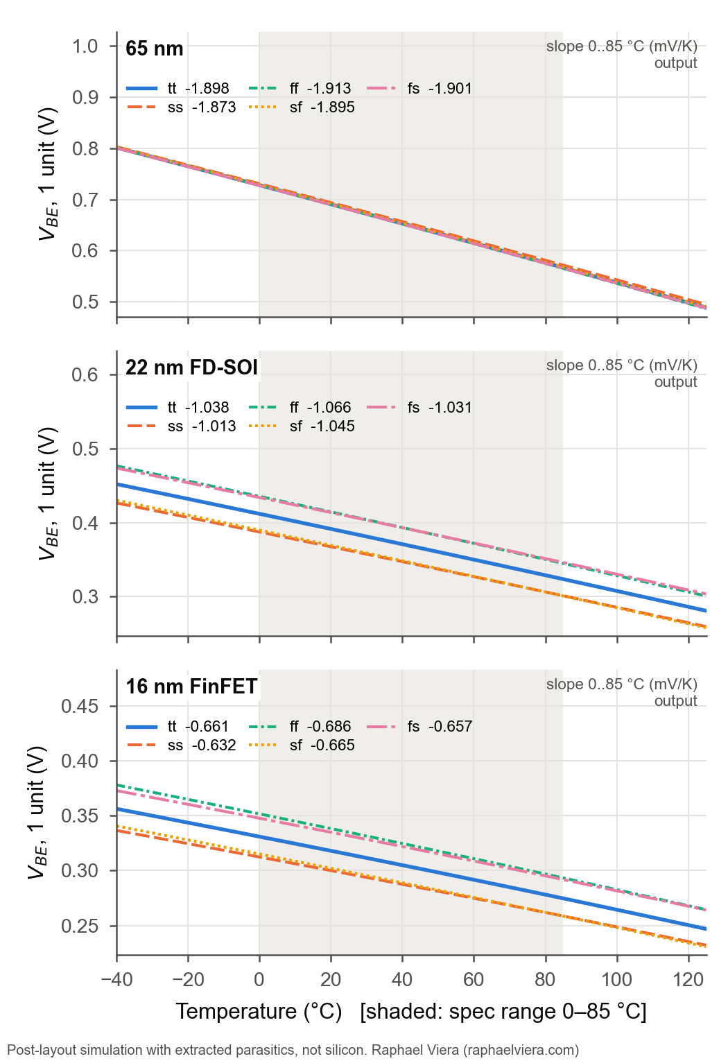
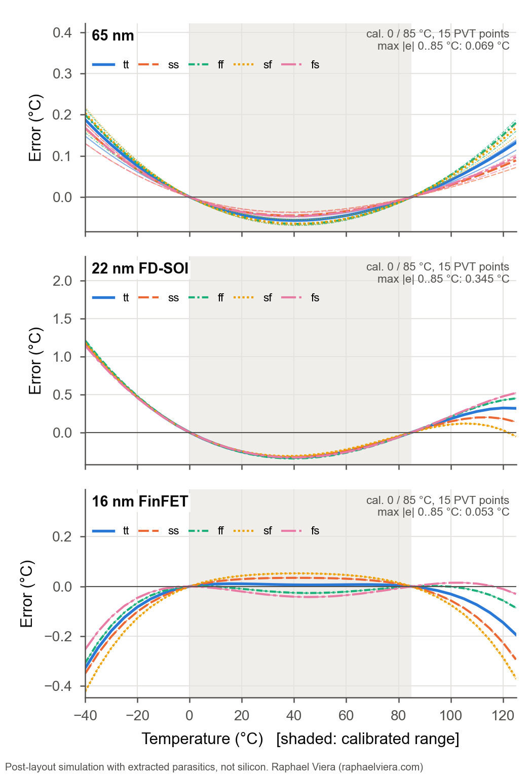
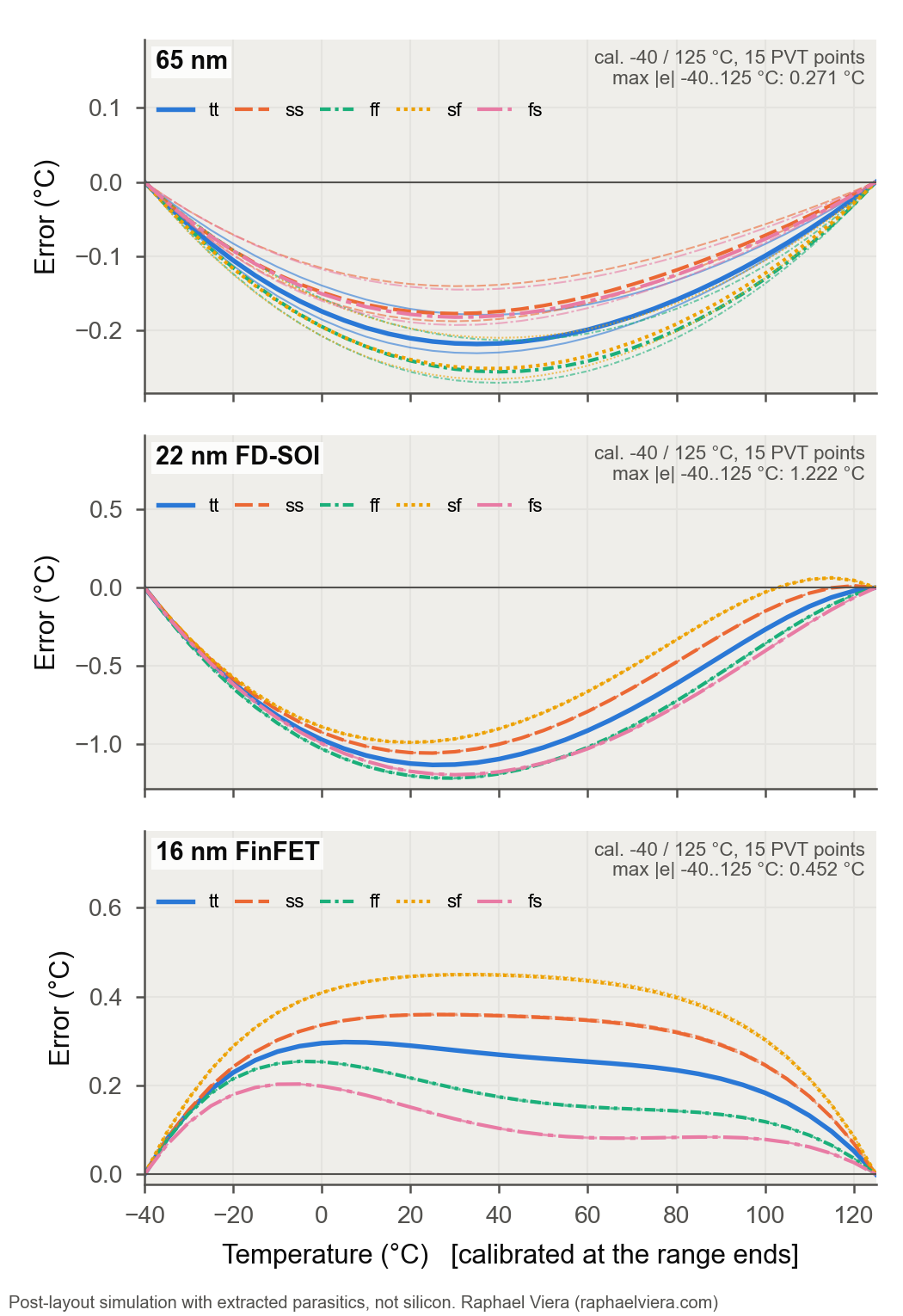
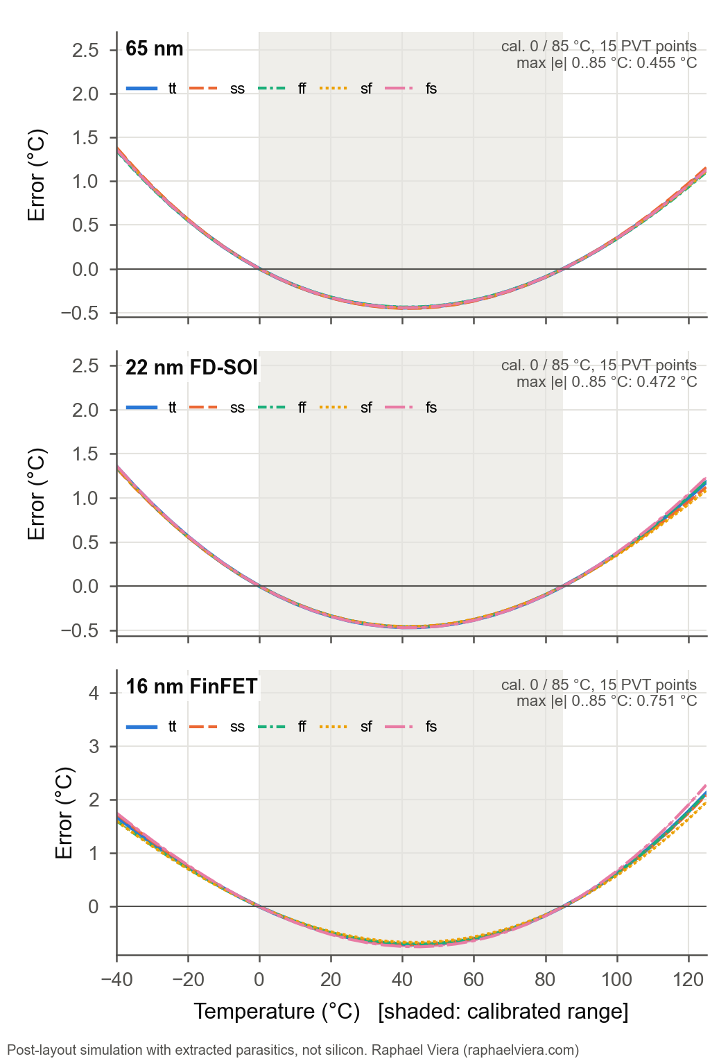
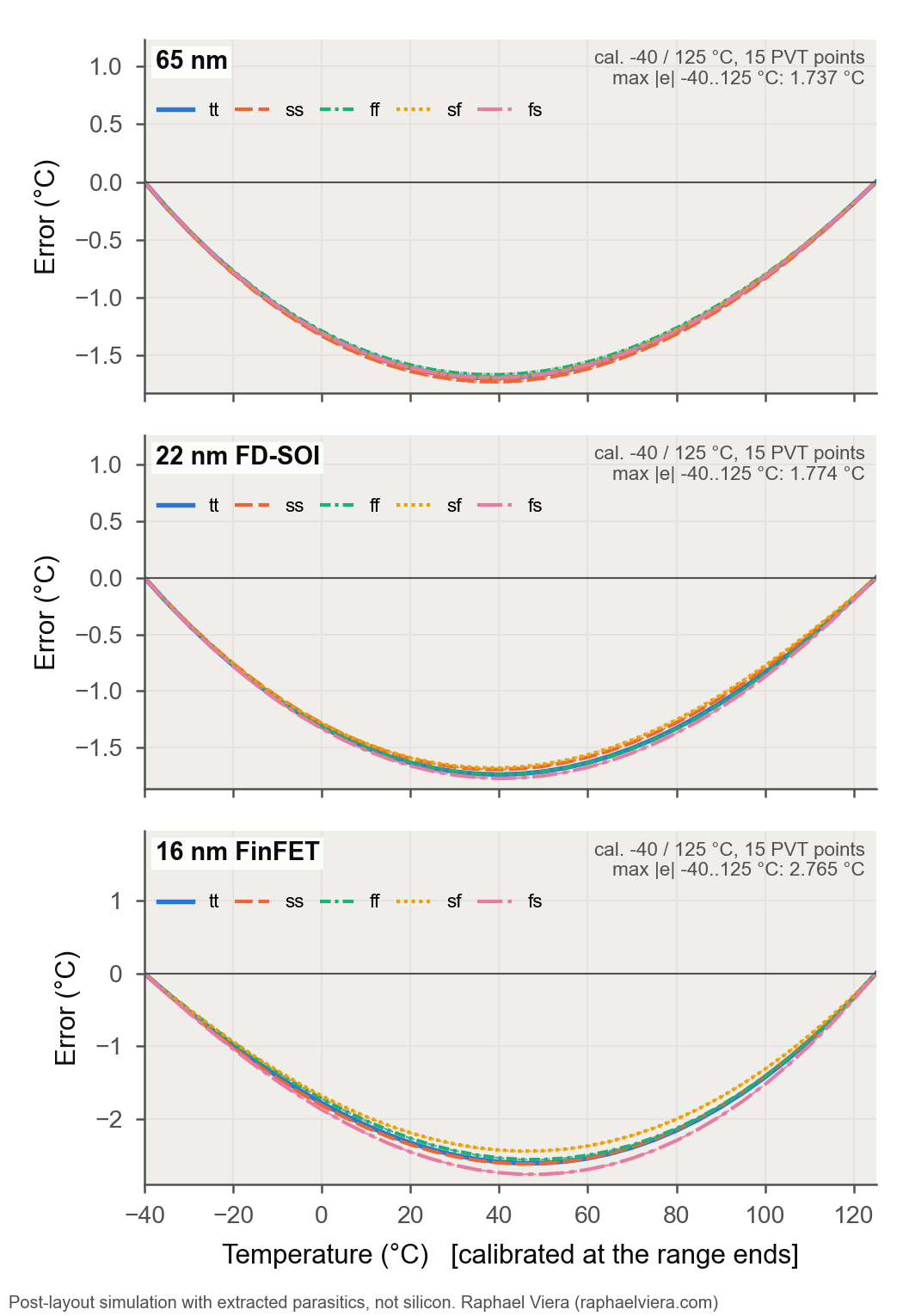
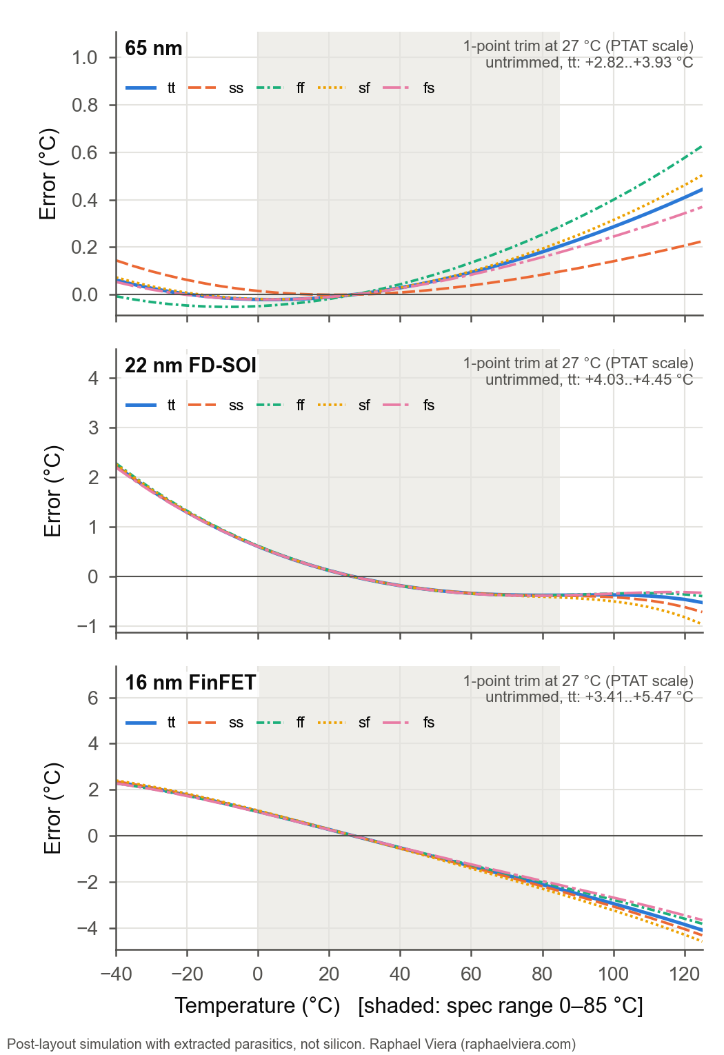
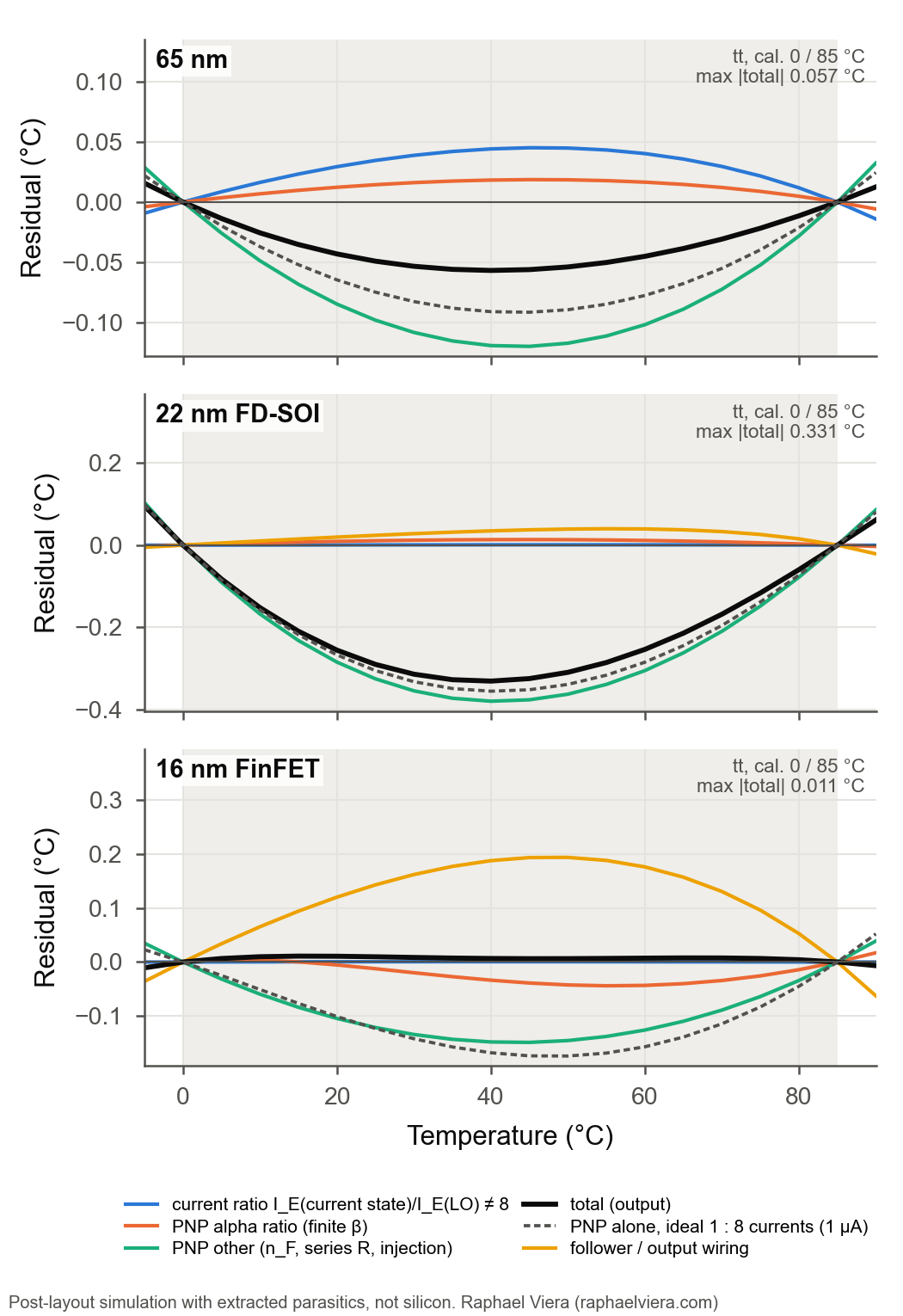
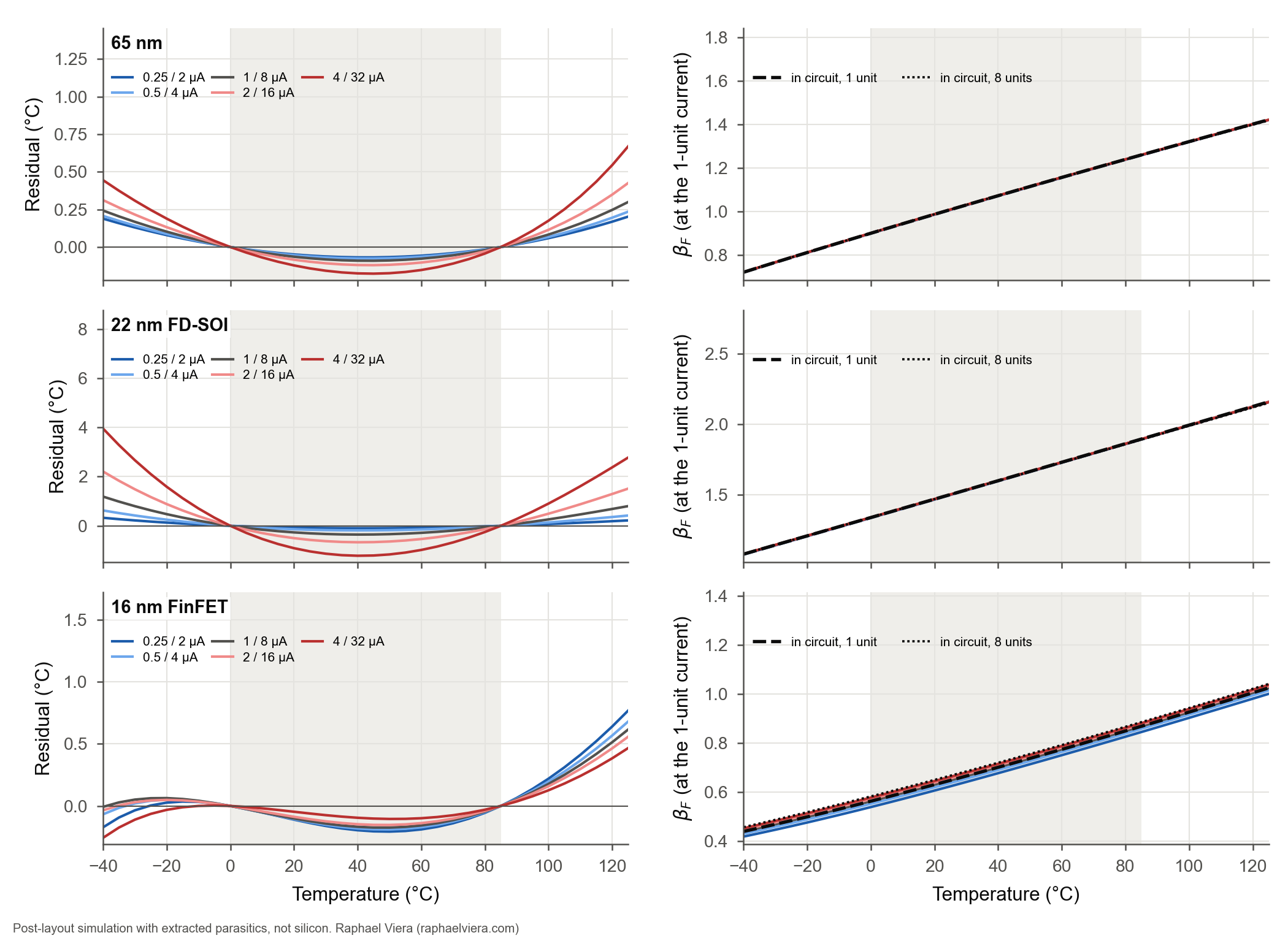
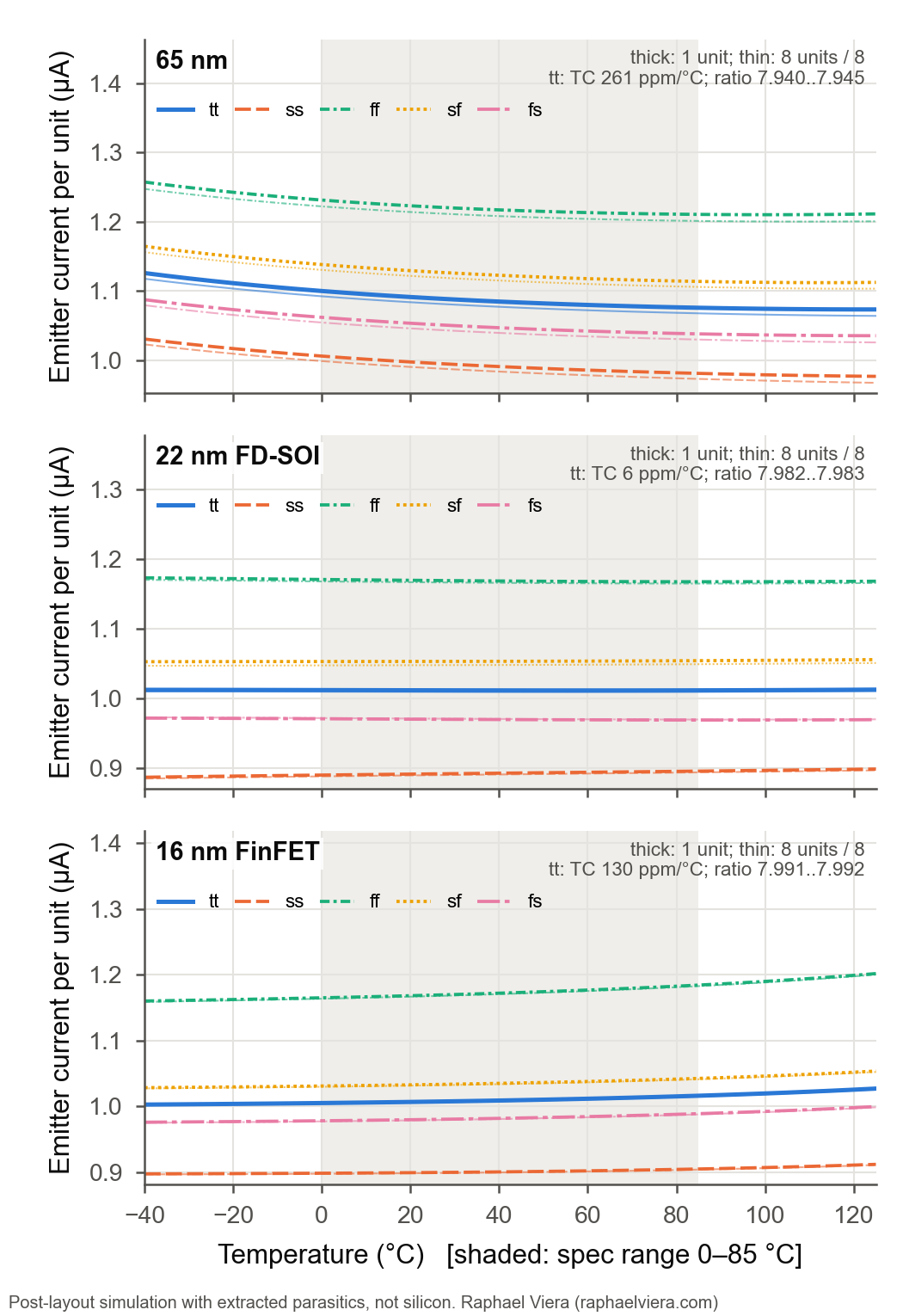
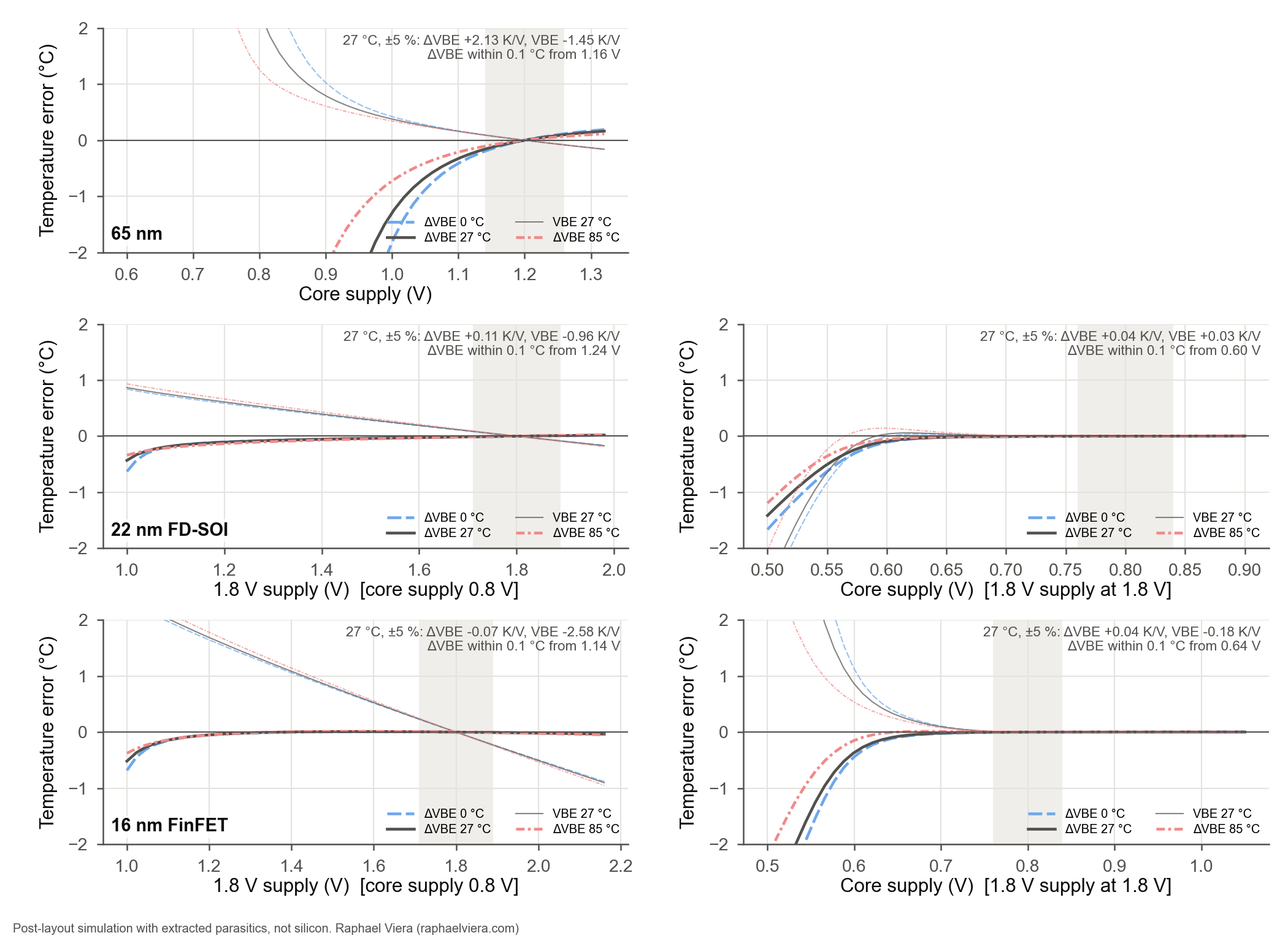
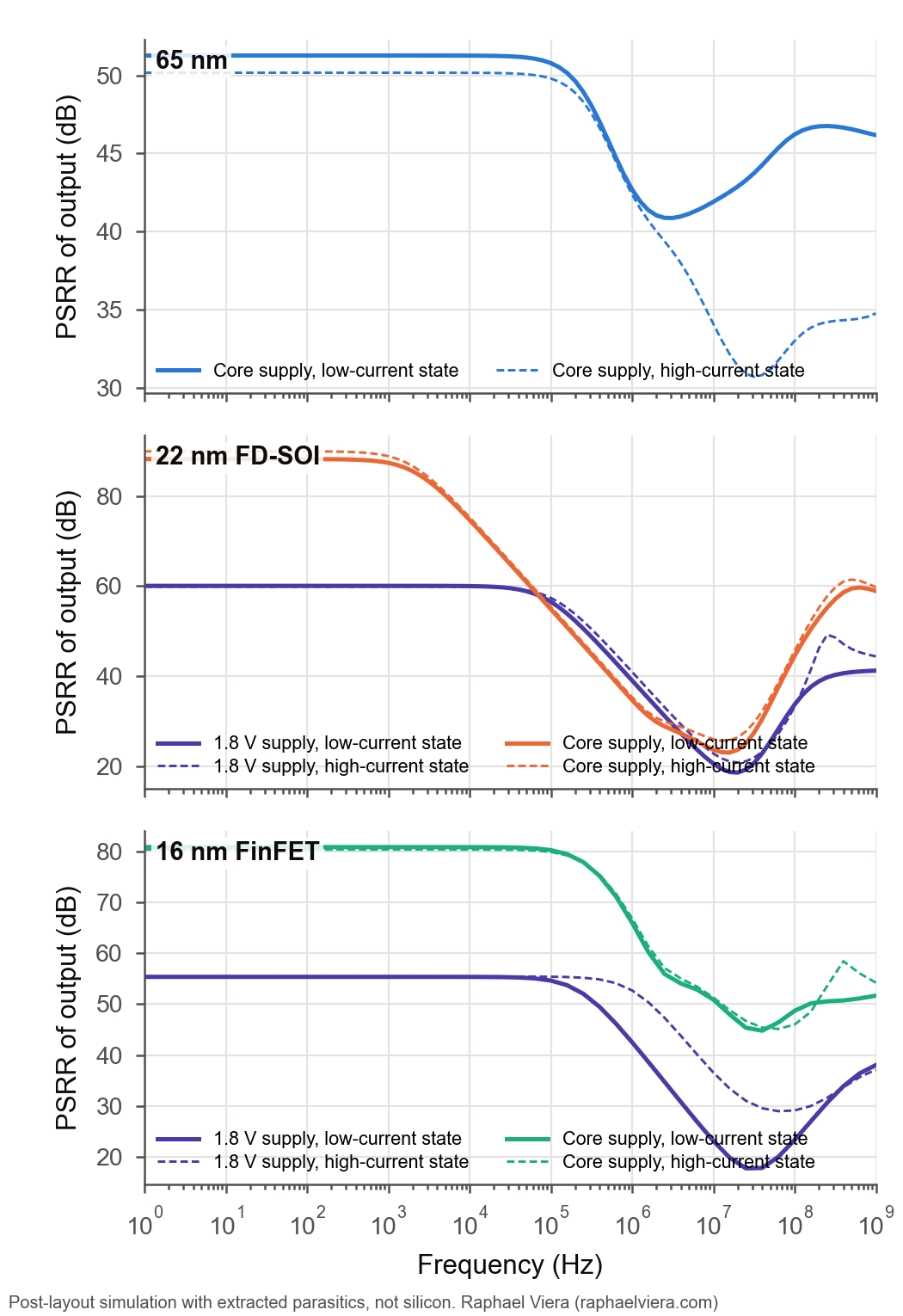
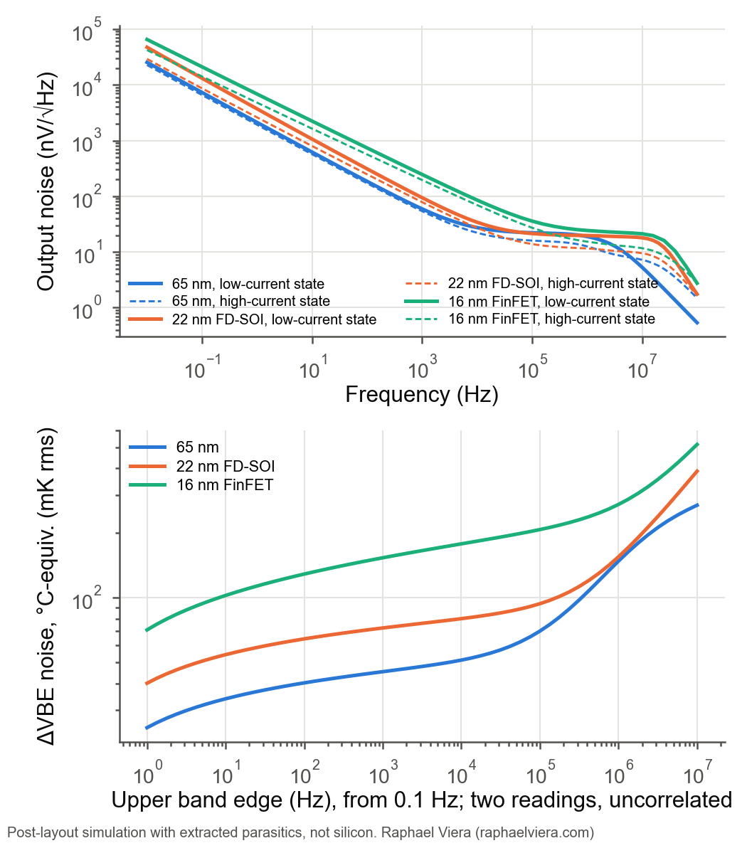
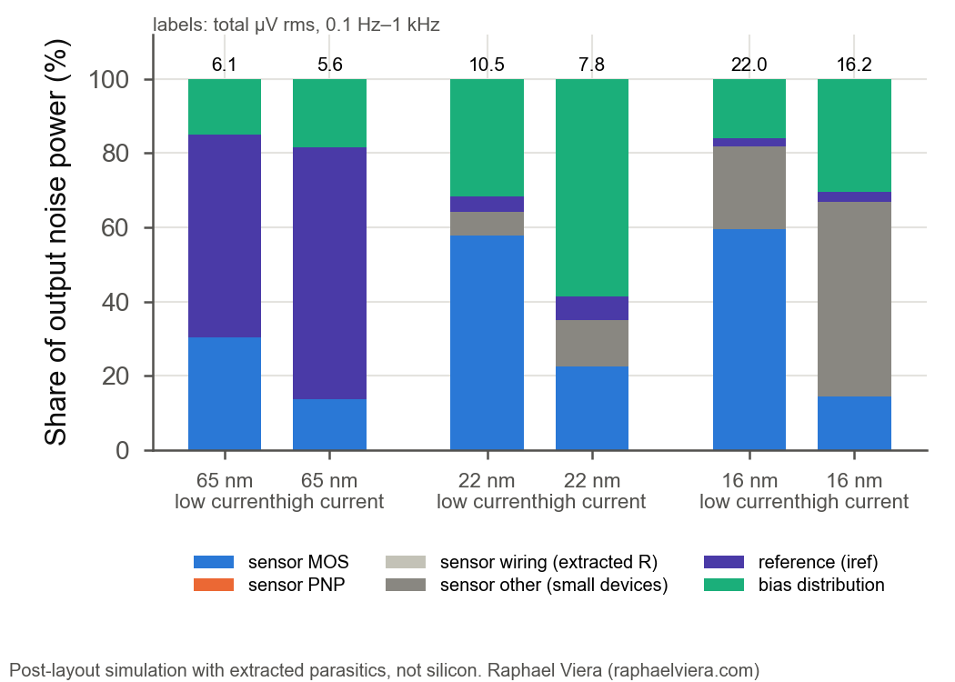
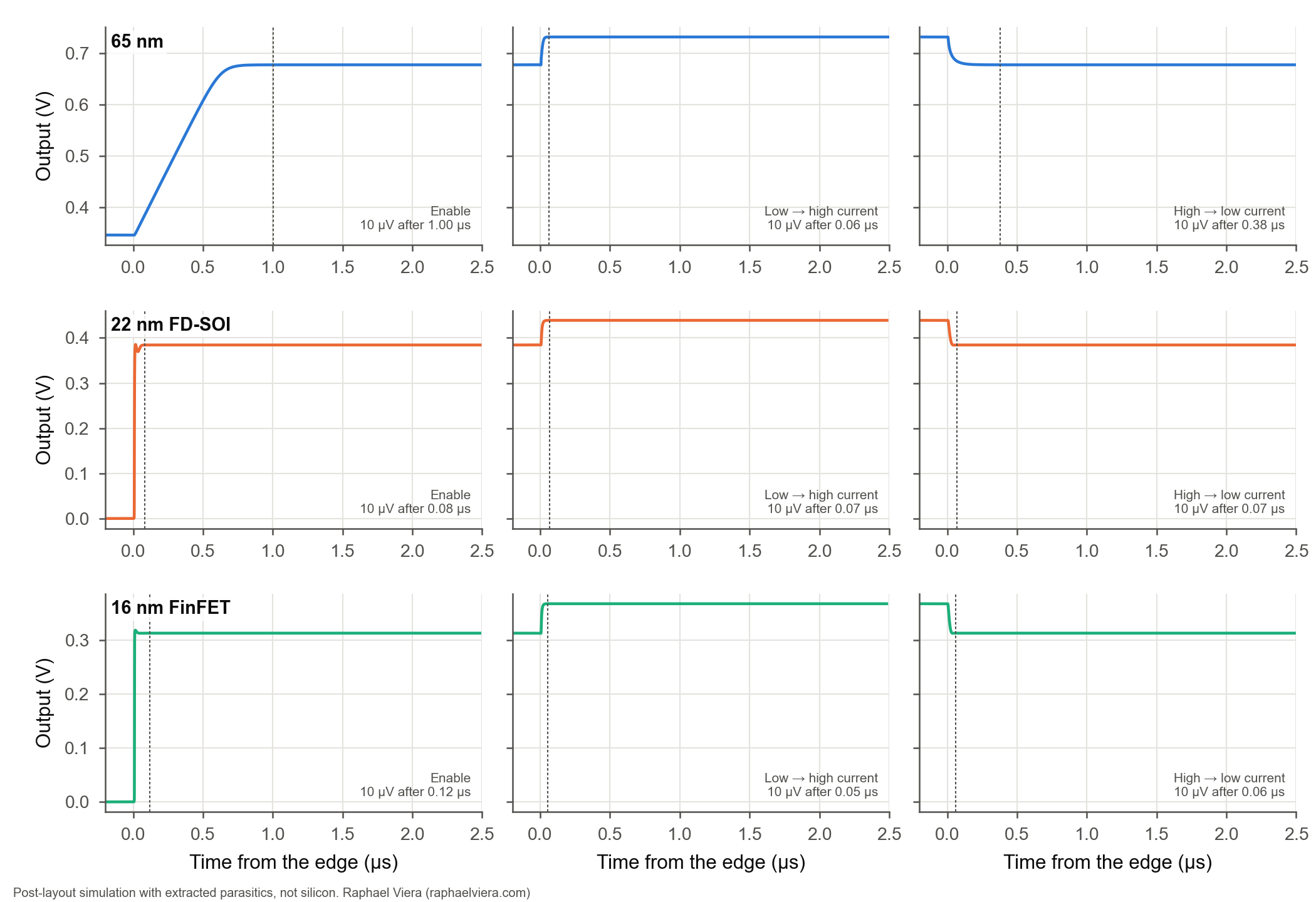
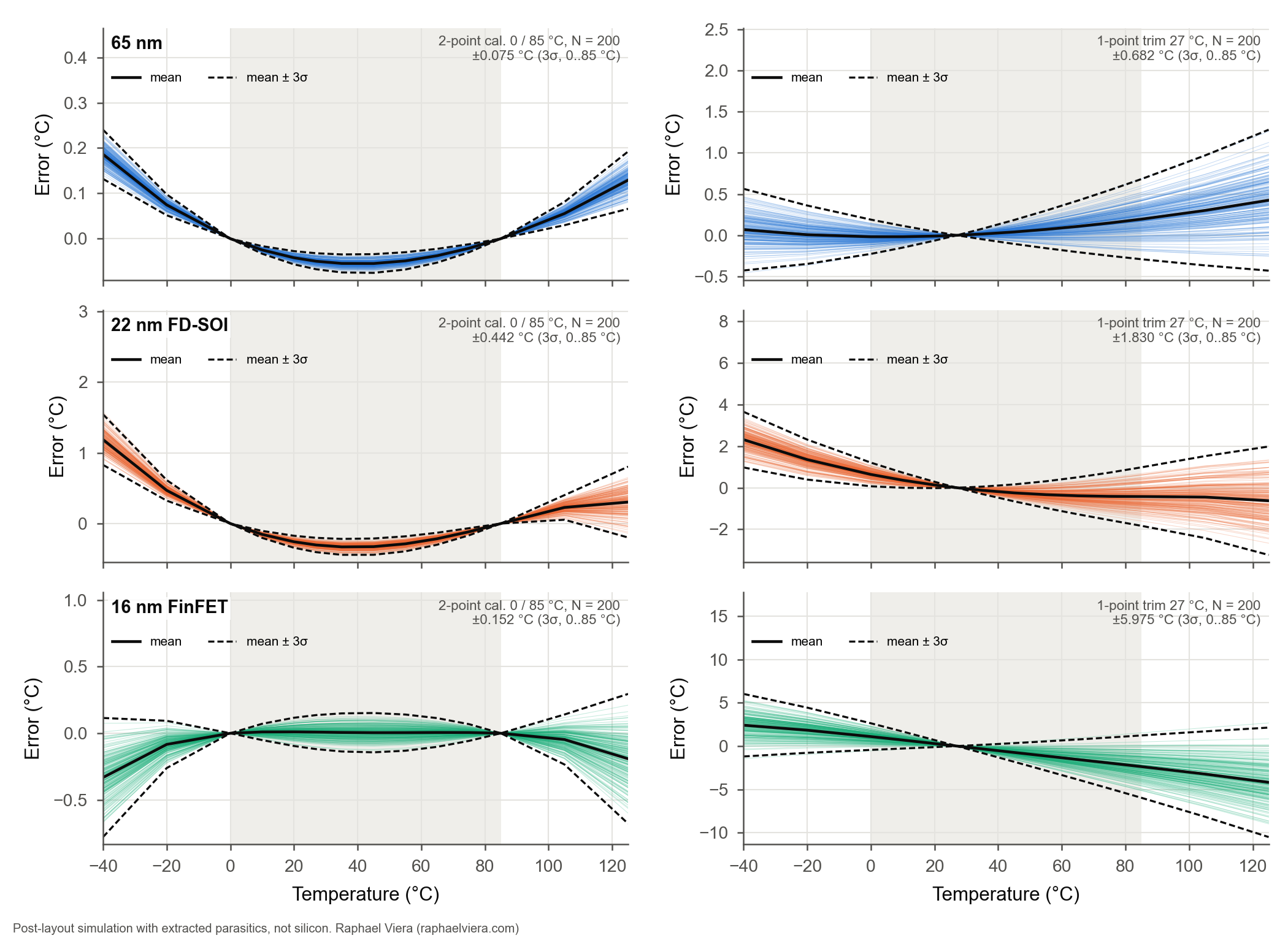
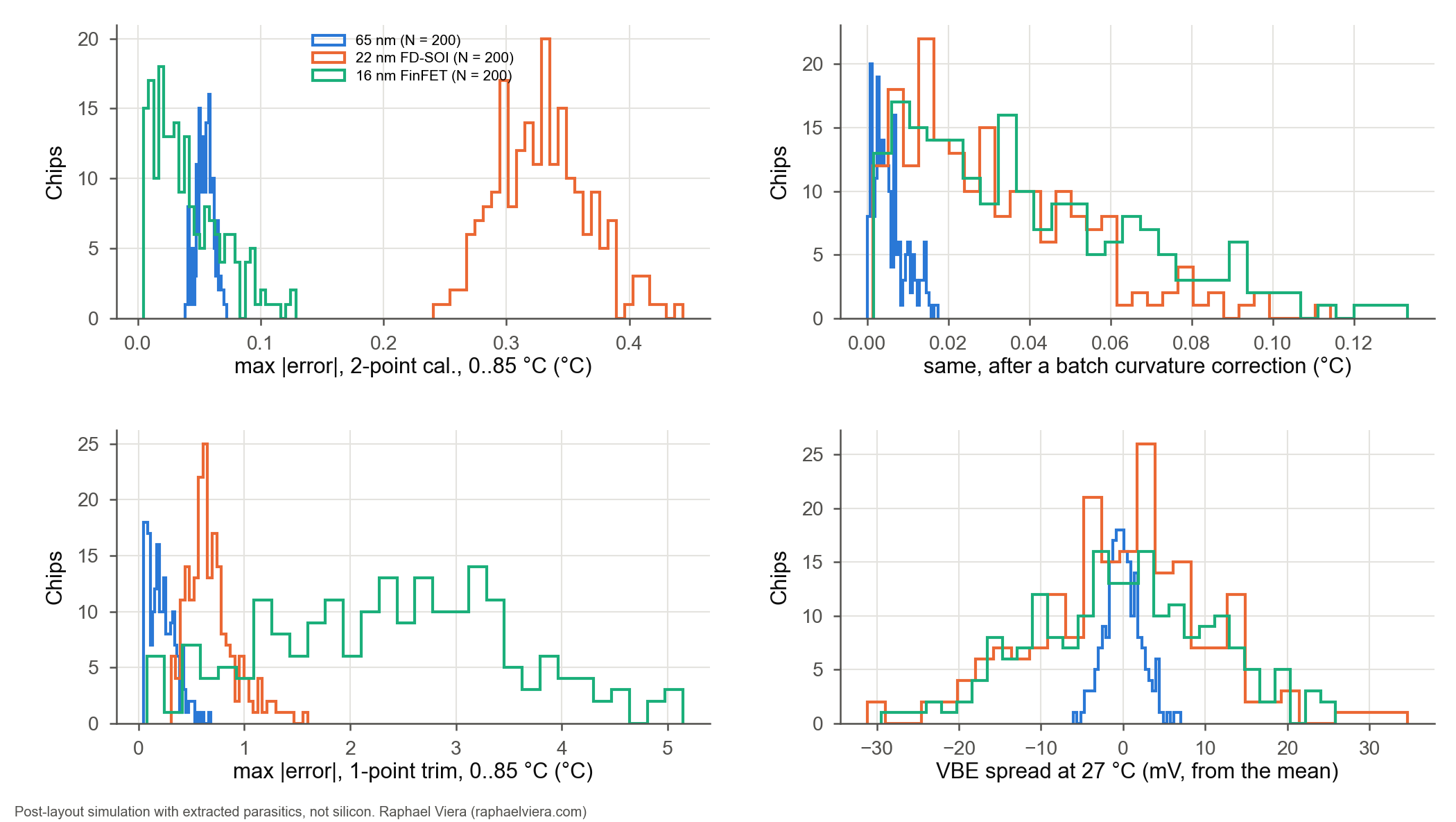
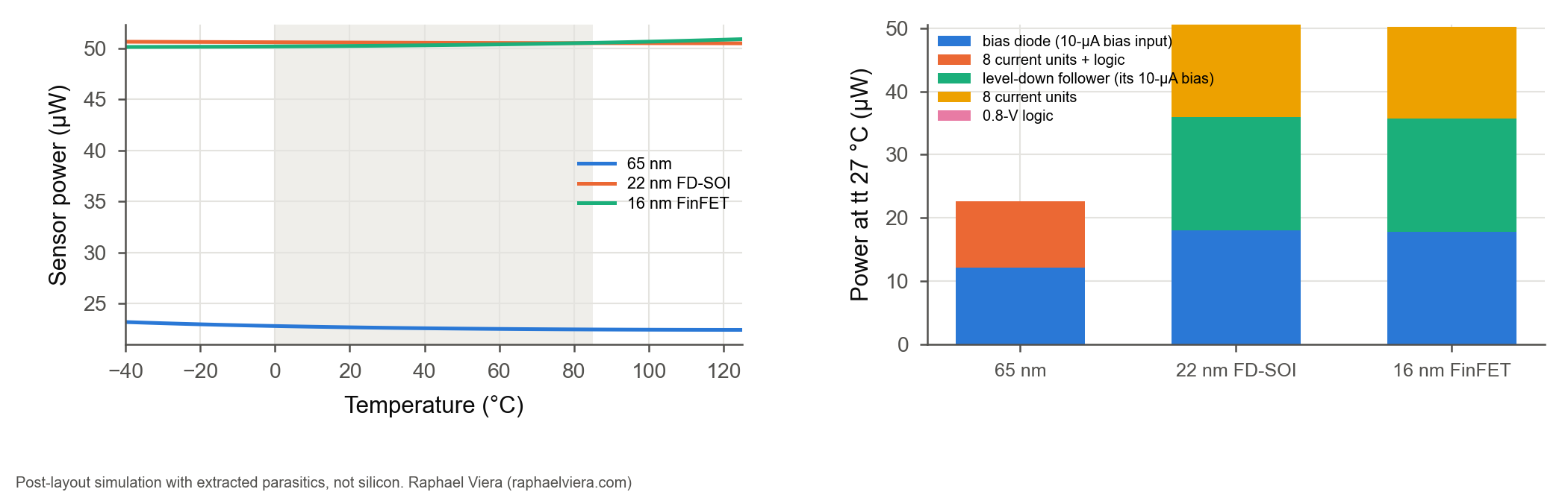
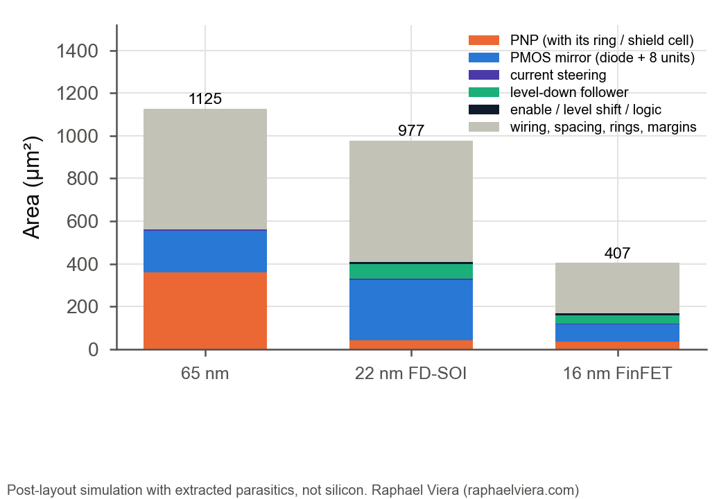
| this work | This work | post-layout | 2026 | 65 nm CMOS | Vertical PNP, switched-current 1 : 8 ΔVBE front end; readout by the chip's shared monitor / ADC (not included) | 0.001125 mm^2 (front end) | 22.6 uW @1.2 V (front end incl. its 10-uA bias) | 0 to 85 (spec); -40 to 125 | ±0.08 (3σ, 2-pt cal. per chip, MC N=200); ±0.68 (3σ, 1-pt trim); −40..125: ±0.29 (2-pt) | front-end noise 45 mK rms (0.1 Hz-1 kHz) | settles in 1.00 us | post-layout simulation, MC 200 | - | this work |
|---|
| this work | This work | post-layout | 2026 | 22 nm FD-SOI | Vertical PNP, switched-current 1 : 8 ΔVBE front end; readout by the chip's shared monitor / ADC (not included); 1.8-V devices + follower | 0.000977 mm^2 (front end) | 50.6 uW @1.8 V (+0.8-V logic) (front end incl. its 10-uA bias and follower) | 0 to 85 (spec); -40 to 125 | ±0.44 (3σ, 2-pt cal. per chip, MC N=200); ±1.83 (3σ, 1-pt trim); −40..125: ±1.60 (2-pt) | front-end noise 72 mK rms (0.1 Hz-1 kHz) | settles in 0.08 us | post-layout simulation, MC 200 | - | this work |
|---|
| this work | This work | post-layout | 2026 | 16 nm FinFET | Vertical PNP, switched-current 1 : 8 ΔVBE front end; readout by the chip's shared monitor / ADC (not included); 1.8-V devices + follower | 0.000407 mm^2 (front end) | 50.3 uW @1.8 V (+0.8-V logic) (front end incl. its 10-uA bias and follower) | 0 to 85 (spec); -40 to 125 | ±0.15 (3σ, 2-pt cal. per chip, MC N=200); ±5.98 (3σ, 1-pt trim); −40..125: ±0.86 (2-pt) | front-end noise 153 mK rms (0.1 Hz-1 kHz) | settles in 0.12 us | post-layout simulation, MC 200 | - | this work |
|---|