Analog building block
Eight matched currents. Three processes.
A 10-µA input drives eight matched 10-µA outputs through a wide-swing cascode mirror adapted to each CMOS technology.
Overview
Eight matched 10-µA outputs in three CMOS technologies.
Physical sign-off
DRC, LVS, antenna, density, latch-up and matched-layout checks.
Reliability review
Electromigration, IR drop, redundant supply vias and gate-oxide voltage.
Extracted-layout verification
PVT, 200-run Monte Carlo and schematic-to-layout comparison.
| Measure | 65-nm bulk | 22-nm FD-SOI | 16-nm FinFET |
|---|---|---|---|
| Macro area | 2,025 µm² | 1,043 µm² | 684 µm² |
| Output matching, worst 1σ | 1.14% | 1.15%¹ | 1.24% |
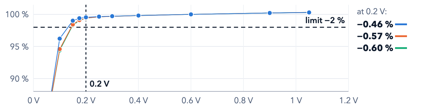
| Output drop at 0.2 V | 0.66% | 1.22% | 1.40% |
| Own power, typical | 1.57 µW | 0.87 µW | 0.96 µW |
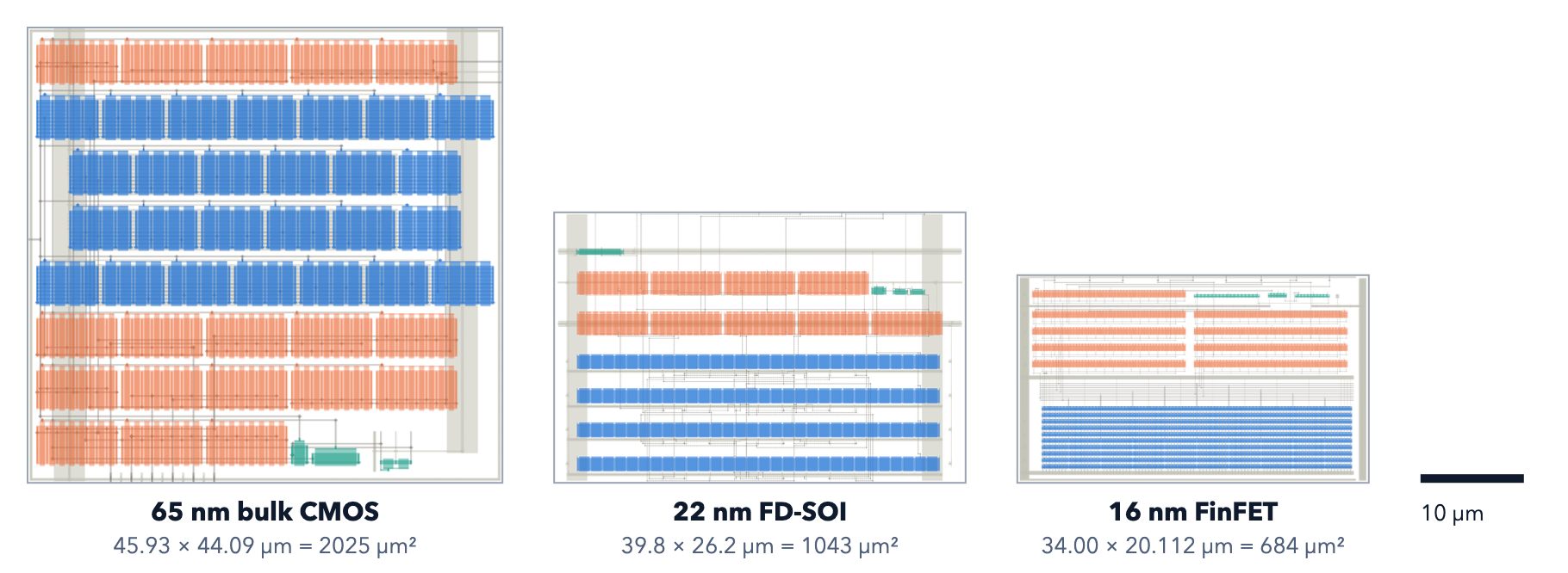
¹The 22-nm design basis uses the best-case matching model; the worst-case model gives 1.94%.
Function & specification
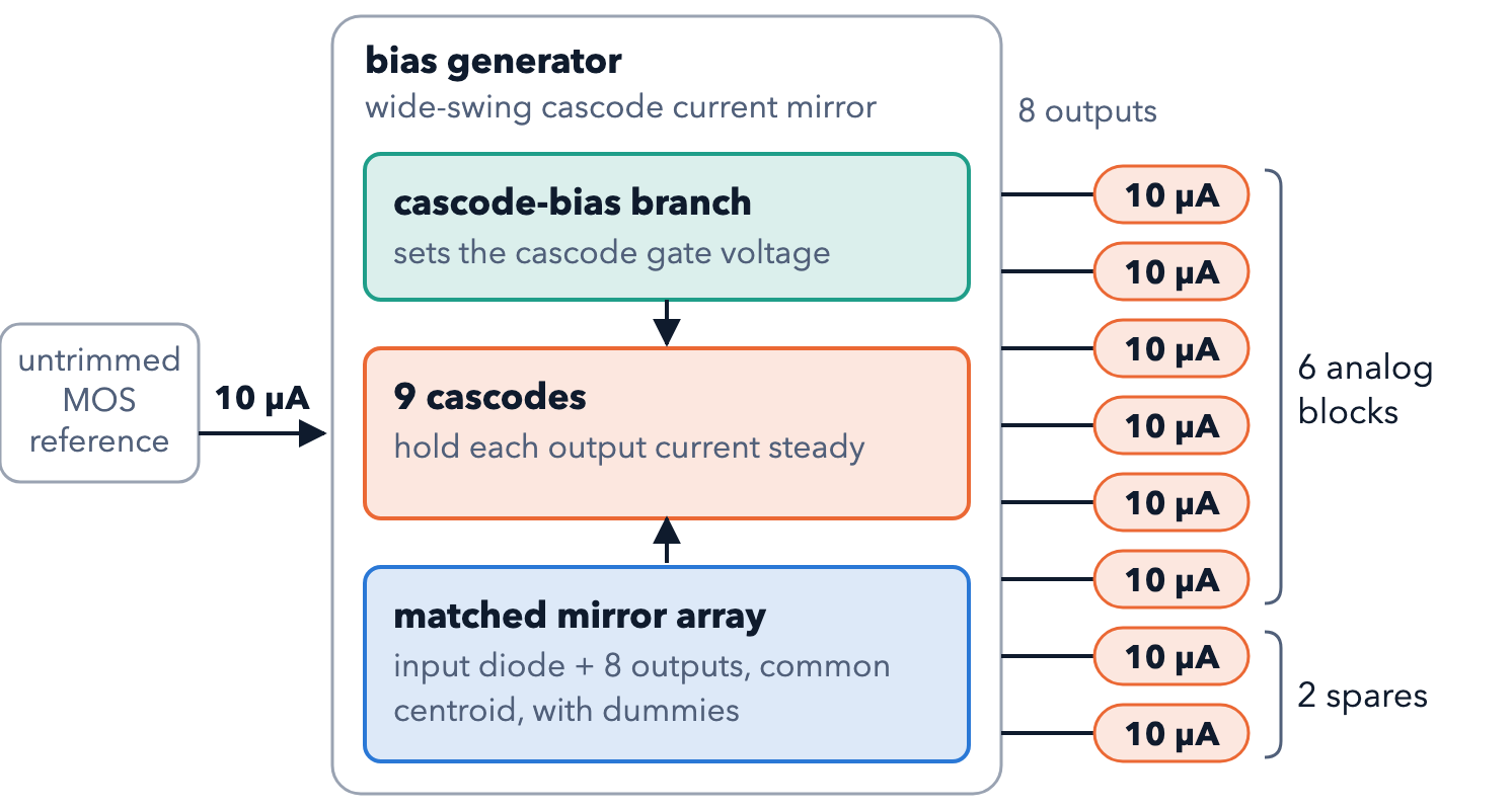
One reference current becomes eight matched bias currents.
| Requirement | Target |
|---|---|
| Supply | 65 nm: 1.2 V; 22 and 16 nm: 0.8 V; all ±5% |
| PVT box | 5 process corners × 0 / 27 / 85 °C × supply ±5% = 45 points |
| Outputs | 8 × 10 µA; each within 2% down to 0.2 V on its pin |
| Output-to-output matching | 1σ ≤ 3% (Monte Carlo) |
| DC supply rejection | ≥ 35 dB |
Transistor schematic
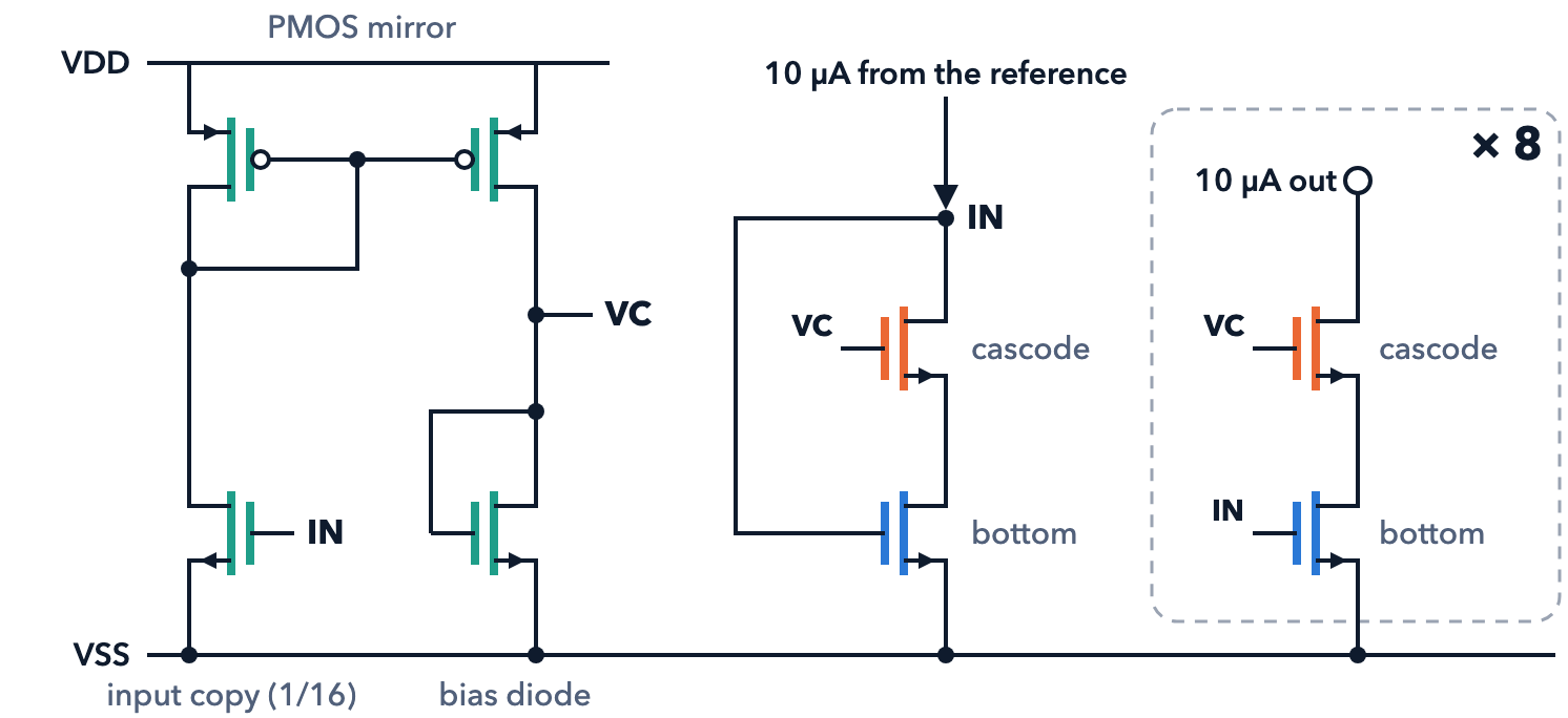
One wide-swing cascode mirror, process-specific device sizing.
| Device group | 65 nm | 22 nm | 16 nm |
|---|---|---|---|
| Bottom devices | 30 / 1 µm, 2 × 4 fingers | 10 / 1 µm, 4 × 2 fingers | 16 × 6 fins, 5 × 192 nm |
| Cascodes | 60 / 0.5 µm, 2 × 8 fingers | 20 / 0.5 µm, 10 fingers | 204 fins, 3 × 168 nm |
| Input copy (1/16) | 1.875 / 1 µm | 0.625 / 1 µm | 6 fins, 5 × 192 nm |
| PMOS mirror | 0.4 / 1 µm | 0.4 / 1 µm | 4 fins, 5 × 192 nm |
| Bias diode | 1.1 / 4 µm | 0.4 / 4 µm | 4 fins, 17 × 240 nm |
Layouts
Signed-off macros shown at one scale.
Matched arrays
Symmetric placement with dummies and equal device surroundings.
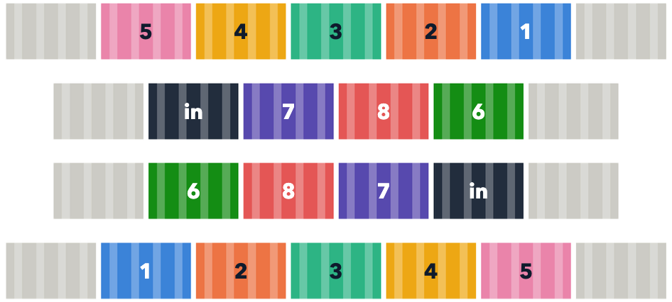
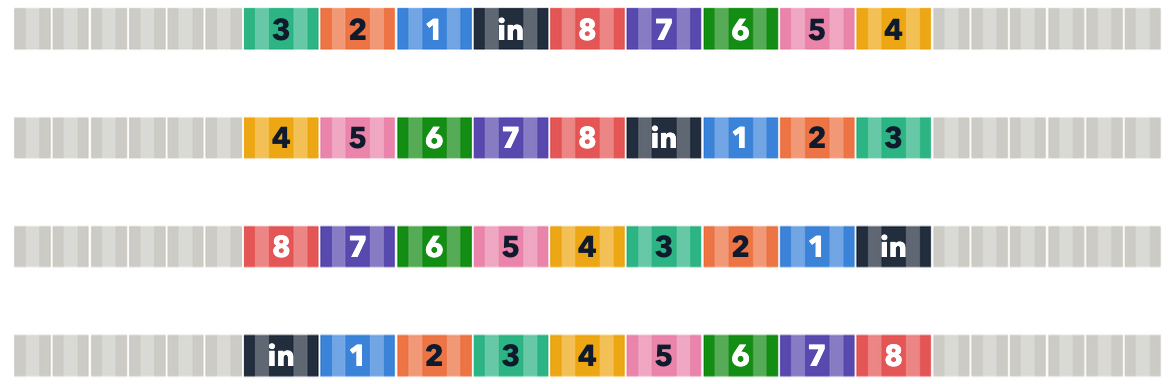
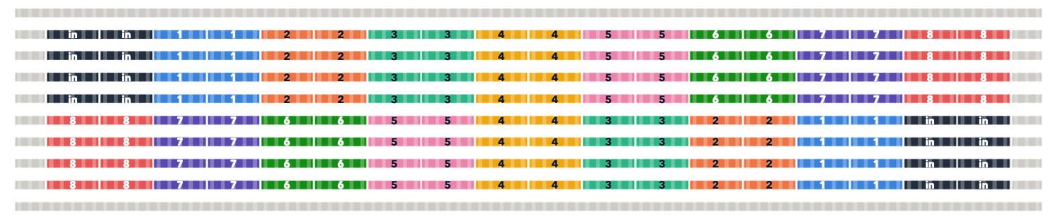
Each output’s units share one drain net; the array map was checked against the drawn connectivity.
Matching
Output-to-output 1σ, one point per output.
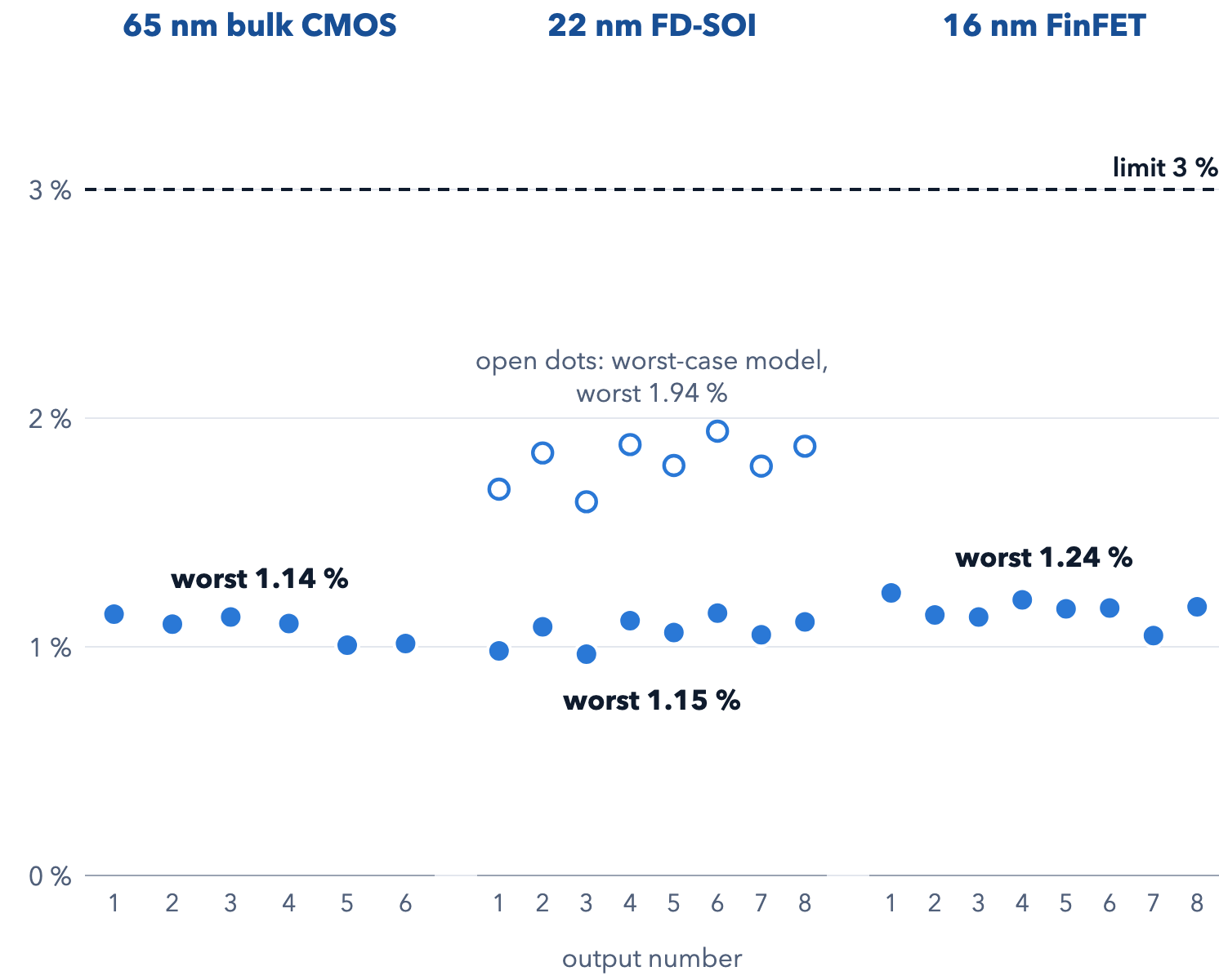
The 65-nm bench included six consumer-loaded outputs; the 22-nm and 16-nm benches included all eight. The target was ≤3%.
Output-voltage sweep by technology
One output per plot, swept from 0 V to the supply; output current is normalized to its value at mid-supply.
65-nm bulk CMOS
22-nm FD-SOI
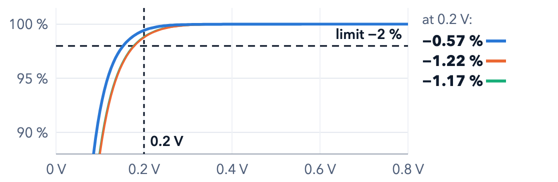
16-nm FinFET
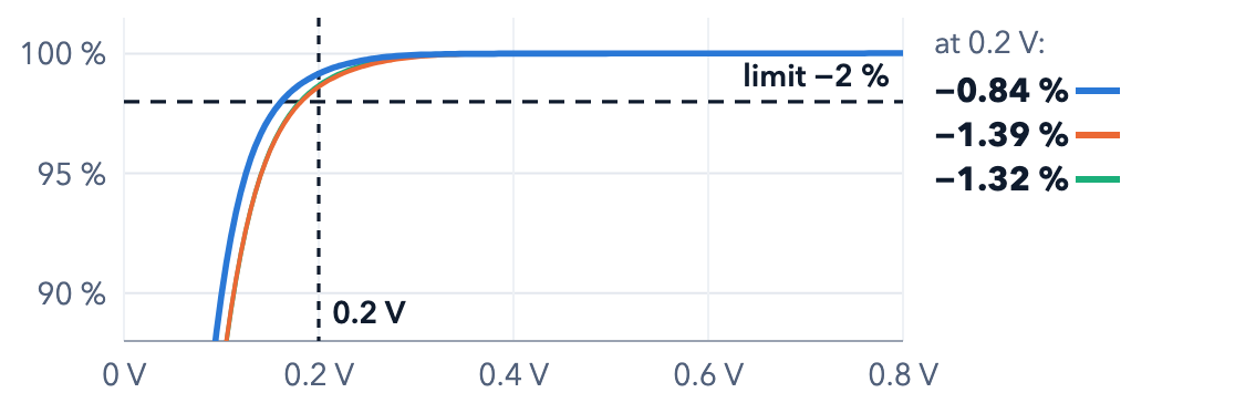
Worst drop at 0.2 V across all 45 PVT points: 0.66%, 1.22% and 1.40% for 65, 22 and 16 nm, respectively. The acceptance target is no more than 2% below the mid-supply current.
Supply rejection
Both the isolated block and the reference-fed chain matter.
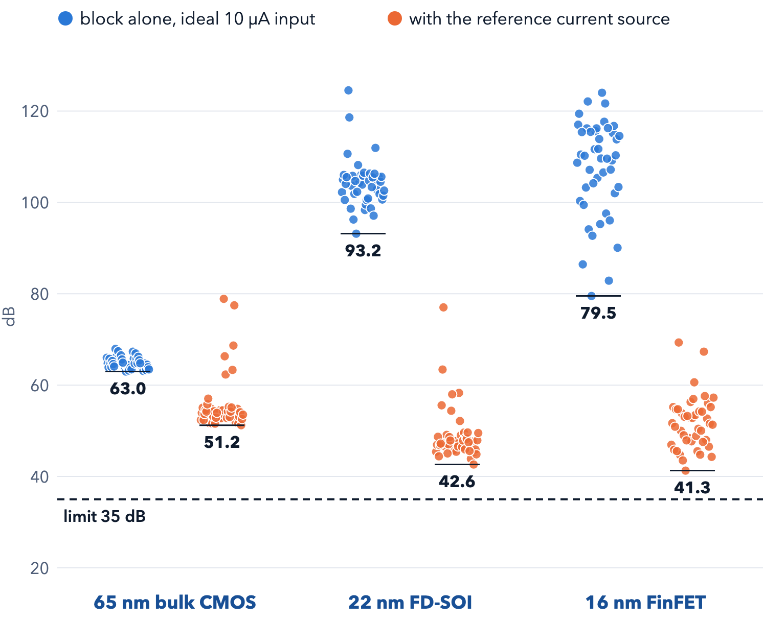
Worst block-alone PSRR: 63.0 / 93.2 / 79.5 dB (65 / 22 / 16 nm). With the reference: 51.2 / 42.6 / 41.3 dB. The acceptance target was ≥35 dB.
Values are post-layout simulation with extracted parasitics, not silicon measurements. Matching is worst-output 1σ at the typical corner and nominal supply. · Raphael Viera (raphaelviera.com)